Circuit description new circuits
GB 50
L9.2E
9.
•
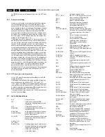
Pin 8: not connected
•
Pin 9: Vst, tuning v33V
•
Pin 10: ground
•
Pin 11: IF, asymmetrical IF output
Note: The +5V supply voltage and the +33V tuning voltage is
derived from the line output stage, see diagram A2).
9.5.3
IF band pass filter (SAW FILTER)
Between the tuner output and the video IF input of the video
processor the IF band pass filtering take place. For the IF band
pass filtering SAW filters are used (item 1003 or 1005). 5 Types
of SAW filters are used depending on the version of the set.
9.5.4
Video IF
General: Video IF-demodulation is achieved in combination
with reference circuit L5006 connected at pin 3 and 4 of
IC7250-A. The AGC control for the tuner is applied via pin 54
of IC7250-A. Internally the IC uses the top sync level as a
reference for AGC control. The AGC adjustment can be
readjusted via the SAM (service alignment menu). C2201
connected to pin 53 determines the time constant of the AGC.
The Base band CVBS signal is present at pin 6 of IC7250-A
(normal amplitude 3.2Vpp). From here the signal is fed via
transistor 7266 to the sound trap filters and then on to the video
source selection circuit.
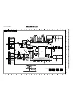
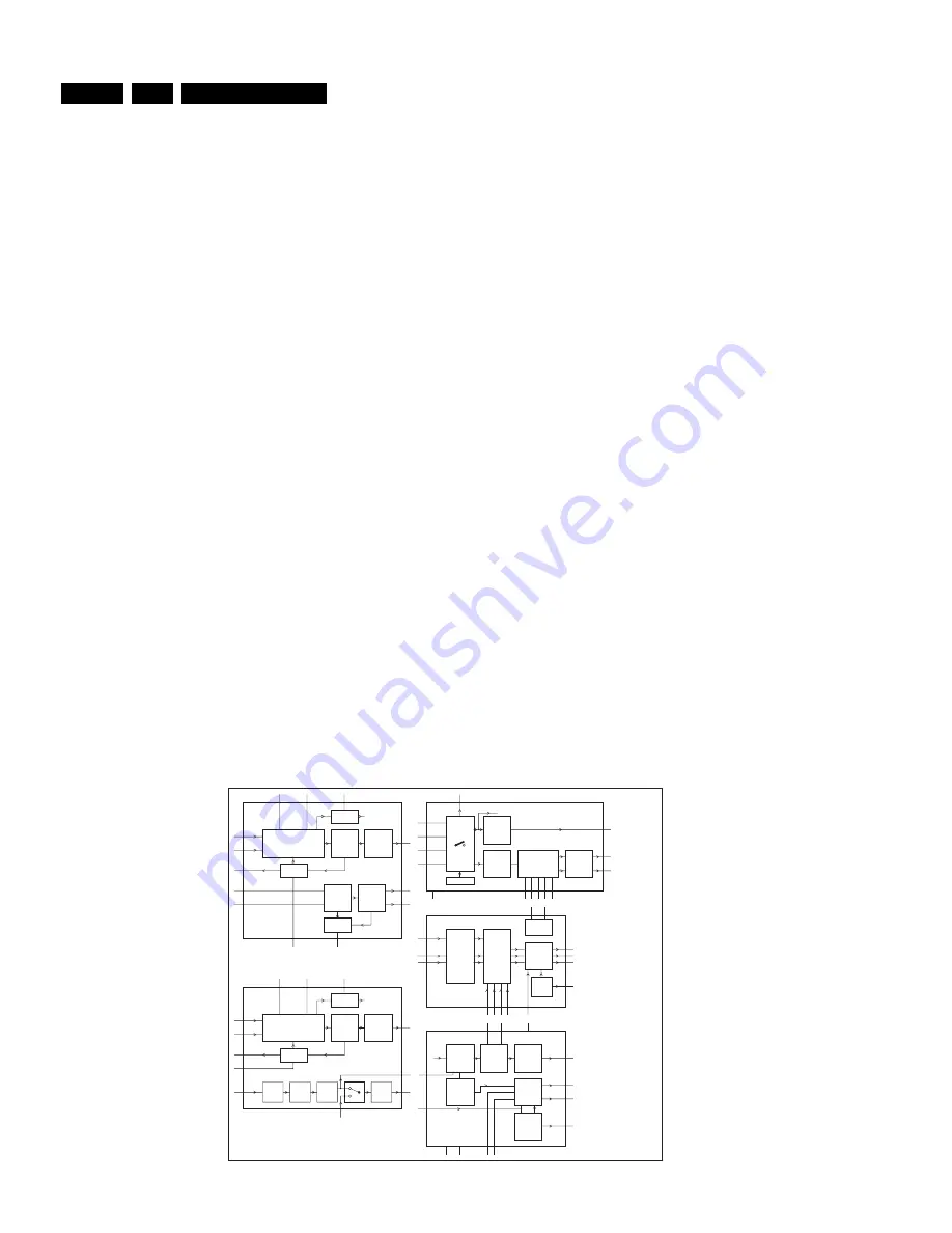
The main functions of the video IF part are (see also figures
9.5):
•
IF- amplifier
•
PLL-demodulator
•
Video buffer
•
AFC
•
IF-AGC
•
Tuner AGC
9.5.5
IF- amplifier
The IF-amplifier incorporates symmetrical inputs (pins 48 and
49). By using IIC bus control (IFS) the AGC attenuation can be
adjusted by up to -20dB.
Remark: If the BIMOS is replaced the AGC value should be
adjusted as part of the repair process. ( see Ch 8 - Alignments
).
9.5.6
PLL-demodulator
The IF-signal is demodulated with the assistance of the PLL
detector. The video IF-demodulator can handle both negative
and positively modulated IF signals; selection is achieved via
the IIC bus (bit MOD).
9.5.7
Video buffer
The video buffer is present to provide a low ohmic video output
with the required signal amplitude. Additionally, it provides
protection against (pin 6) the occurrence of noise peaks. The
video buffer stage also contains a level shifter and a gain stage
for both the positive and negative video modulation formats, so
that the correct video amplitude and DC level are always
present at pin 6 regardless of the input signal.
9.5.8
Video-IF AGC
An AGC system controls the gain of the IF amplifier such that
the video output amplitude is constant. The demodulated video
signal is supplied, via a low pass filter inside the IC to an AGC
detector. External AGC de coupling is provided by capacitor
2201 at pin 53. The AGC detector voltage directly controls the
IF amplification stages.
9.5.9
The tuner AGC
Tuner AGC is provided to reduce the tuner gain and thus the
tuner output voltage when receiving to strong RF signal. The
tuner AGC starts working when the video-IF input reaches a
certain input level. This level can be adjusted via the IIC bus.
The tuner AGC signal is applied to the tuner via the open
collector output pin 54 of the BIMOS.
9.5.10 AFC
The AFC output information is available for search tuning. The
AFC output is available via the I2C bus ( AFA and AFB signals).
For alignment purposes it is displayed in the TUNER submenu
of the SAM (See chapter 8).
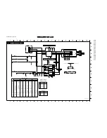
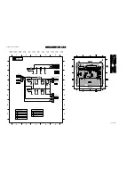
Figure 9-14 “BIMOS”
IC 7250-4A
TDA 8845
7250-4B
TDA 8844/45
7250-4C
TDA 8844/45
7250-4D
TDA 8844/45
IC 7250-4A
TDA 8844
AGC
AGC
SOUND
IF
AMPL.
QSS MIXER
+
SOUND
AM DEM.
AFC
AFC
VIDEO
AMPL.
VIDEO-
BASE-
BAND
OUTPUT
IF AMPLIFIER
+
PLL VIDEO DEMO.
54
49
48
3
4
5
6
AGC
AFC
AFC
VIDEO
AMPL.
VIDEO-
BASE-
BAND
OUTPUT
IF AMPLIFIER
+
PLL VIDEO DEMO
54
49
48
3
4
5
6
55
55
1
1
2
2
56
15
15
53
53
LIMITER
PLL-
AUDIO
FM DEMO.
AMPL.
+
MUTE
OUTPUT
+
VOLUME
CONTROL
16
9
36 35 34 33
PAL/NTSC/
SECAM
DEMODULATOR
CHROMA
BANDPASS
BASE-
BAND
DELAY
LINE
LUM.
DELAY
PEAKING
CORING
28
29
30
13
17
10
11
38
VIDEO IDENT
Y (TO SYNC PART)
CD MATRIX
+
SATURATION
CONTROL
+
SKIN
TINT
27
31
32
7
8
21
20
19
18
22
23 24 25 26
Y
U
V
RGB
MATRIX
+
BLACK
STRETCH
+
RGB1
INPUT
IIC BUS
CONTROL
R
G
B
R
G
B
RGB
OUTPUT
CATH.
CALIB.
41
42
37
SYNC.
SEPARATOR
VCO
+
CONTROL
HORIZONTAL
OUTPUT
VERTICAL
OUTPUT
E/W
OUTPUT
VERT.
SYNC.
SEPARATOR
Y
43
50
40
46
47
45
52
51
44
39
CL 86532104_021.EPS
220299
OR
INPUT SELECT
Y + CHROMA
PROCESSING
RGB
OUTPUT
SYNC
Содержание L9.2EAA
Страница 5: ...Directions for use GB 5 L9 2E 3 3 Directions for use ...
Страница 6: ...Directions for use GB 6 L9 2E 3 ...
Страница 7: ...Directions for use GB 7 L9 2E 3 ...
Страница 31: ...Schematics and PWB s GB 31 L9 2E 7 ...
Страница 32: ...Schematics and PWB s GB 32 L9 2E 7 ...
Страница 38: ...Schematics and PWB s GB 38 L9 2E 7 ...
Страница 42: ...Schematics and PWB s GB 42 L9 2E 7 Personal notes Personal notes ...

