Circuit-, IC Descriptions and List of Abbreviations
EN 151
DVDR880-890 /0X1
9.
9.3.2
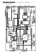
Power Supply Unit
Functional Principle:
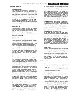
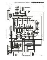
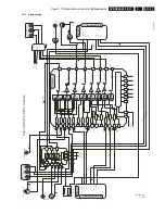
This power supply works in the way of a flyback converter. In
the mains input part [1931 to 2309], the mains voltage is recti-
fied and buffered in the capacitor [2309]. From this direct volt-
age at [2309] energy is transferred into the transformer [5300,
pins 7-5] during the conductive phase of the switching transis-
tor [7307] and is stored there as magnetic energy. This energy
is passed to the secondary outputs of the power supply in the
blocking phase of the switching transistor [7307]. With the
switch-on time of the switching transistor [7307], the energy
transferred in every cycle is regulated in such a way that the
output voltages remain constant regardless of changes in the
load or mains voltage. The power transistor is driven by the
integrated circuit [7313].
Mains input part:
The mains input part extends from the mains socket [1931] to
the capacitor [2309]. The diodes [6301, 6302, 6305 and 6306]
rectify the AC supply voltage, which is then buffered by the
capacitor [2309]. The common mode coil [5302] and capacitor
[2302] work as a filter to block interference arising in the power
supply from the mains. Components [1302], [3306] protect the
power supply against short-term over voltages in the mains,
e.g. caused by indirect lightning.
Start-up with Mains-on:
After connecting the power cord to the mains, the capacitor
[2325] is loaded via a current source between pin 8 and pin 1
in the IC [7313]. Once the voltage on [2325] and therefore the
supply voltage V
cc
of the IC [7313] has reached approx. 11V,
the IC starts up and provides pulses at its output pin 5. These
pulses are used to drive the gate of the power transistor
[7307]. The frequency of these pulses is depending on load
and mains voltage. The current consumption of the IC is
approx. 5 mA at V
cc
in normal mode.
If V
cc
drops to below approx. 9V (e.g. with power limitation) or if
V
ac
exceeds approximately 16V (e.g. interruption of the control
loop), the output of the IC [7313, pin 5] is blocked and a new
start-up cycle begins. (See also “Overload, Power Limitation,
Burst Mode“ section)
Normal operation:
With increasing load on one or more of the power supply out-
puts, the switch-on time for the power transistor [7307]
increases, and thus also the peak value of the delta-shaped
current through this power transistor. The equivalent voltage of
this current profile is passed from resistors [3321] and [3352]
via [3365] to pin 5 of the IC [7313]. If the voltage on pin 2
reaches approx. 0.4V in one switching cycle, the conductive
phase of the switching transistor is ended immediately. The
check is done in each individual switching cycle. This process
ensures that no more than approx. 50W can be taken out from
the mains ( =
power limitation
).
If the power supply reaches the power limit, the output volt-
ages and the supply voltage V
cc
on pin 1 of the IC [7313] will
be reduced following further loading. If V
cc
is less than approx.
9V at any point during this process, the output of the IC [7313,
pin 6] is blocked. All output voltages and V
cc
decrease and a
new start-up cycle begins. If the overload status or short-cir-
cuit remains, the power limitation will be activated immediately
and the voltages will again decrease, followed by another
start-up cycle (
Burst Mode
). The amount of power taken up
from the mains in burst mode is low.
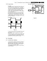
Overload, power limitation, burst mode
With the power supply in normal mode, the periodic
sequences in the circuit are divided primarily into the conduc-
tive and blocking phase of the switching transistor [7307]. Dur-
ing the
conductive phase
of the switching transistor [7307],
current flows from the rectified mains voltage at capacitor
[2309] through the primary coil of the transformer [5300, pins
7-5], the transistor [7307] and resistors [3321, 3352] to ground.
The positive voltage on pin 7 of the transformer [5300] can be
assumed as constant for a switching cycle. The current in the
primary coil of the transformer [5300] increases linearly. A
magnetic field representing a certain value of the primary cur-
rent is formed inside the transformer. In this phase, the volt-
ages on the secondary coils are polarized such that the diodes
[6300, 6303, 6307, 6308, 6310, 6313, 6317 and 6319] block.
From the controller [7315] a current is supplied into the CTRL
input on the IC [pin 3, 7313] via optocoupler [7314]. Once the
switch on time of the switching transistor [7307] - that corre-
sponds to the current supplied into the CTRL input - has been
reached, the switching transistor [7307] is switched off.
When the switching transistor has been switched off, the
blocking phase
begins. No more energy will be transferred
into the transformer. The inductivity of the transformer will still
attempt to keep the current flowing at a constant level (U=L*di/
dt). Switching off transistor [7307] interrupts the primary cur-
rent circuit. The polarity of the voltages on the transformer is
reversed, which means that the diodes [6300, 6303, 6307,
6308, 6310, 6313, 6317 and 6319] become conductive and
current flows into the capacitors [2305, 2312, 2319, 2322,
2326 and 2328] and the load. This current is also ramp-
shaped (di/dt negative, therefore decreasing).
The
feedback control
for the switched-mode power supply is
done by changing the conductive phase of the switching tran-
sistor so that either more or less energy is transferred from the
rectified mains voltage at [2309] into the transformer. The reg-
ulation information is provided by voltage reference [7315].
This element compares the 5V-output voltage via voltage
divider [3332, 3333, 3334] with an internal 2.5V reference volt-
age. The output voltage of [7315] passes via an optocoupler
[7314] for insulation of primary and secondary parts as a cur-
rent value into pin 3 on the IC [7313]. The switch-on time of the
transistor [7307] is inversely proportional to the value of this
current.
Standby modes:
In the ‘AV-Standby‘ operating mode of the set, the ’ION‘ control
line is primarily used to switch off all output voltages for Basic
Engine and Digital Board (supplies 3V3, 5V, 12V, 5N and 4V6
at Connectors 1932 and 1933) of the power supply. This
reduces the amount of power taken from the mains. In Low
Power Standby mode additionally the ‘STBY’ control line is
used to switch off output voltages 5SW and 8SW. This reduces
power consumption to less than 3W. The power supply will
continue operating in Standby mode with a switching frequency
of approx. 25 kHz.
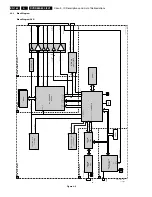
9.3.3
Frontend
This unit is designed to support two basic versions, which are
distinguished by a different assembly variant only (one for mul-
tistandard and the second for Pal-I only) and comprises the
following parts:
•
Tuner UV1316K [1705]
•
IF amplifier & video demodulator IC TDA 9818/9817 [7710]
•
Sound processor MSP3415G [7600]
Tuner and IF selection
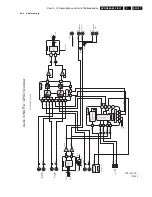
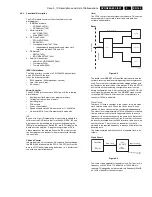
The Tuner [1705] converts the RF-signal coming from the
antenna input to an IF-signal. The tuner is fully controlled via
I²C-bus of the CC-
µ
P. [1705] is also equipped with a “passive-
loop-through” between antenna-in and –out to save power in
stand-by of the set, when the complete part is not supplied.
The IF frequency of the video carrier is 38.9 MHz for all sys-
tems except SECAM L' (34,0 MHz).
A quasi-split audio system is used. Separate surface-wave fil-
ters (SAW) are required. [1701], [1703] for video, [1702] for
audio. [1701] is switched into the signal path for DK/I-SECAM
L/L' reception, if the signal “SFS_TS” is “high”. In this case the
switches [7704], [7705] are open and the diode [6703] is con-
ducting. [1703] is switched into the signal path for BG recep-
tion (“SFS_TS” is “low”). Then the switch [7712] is open and
the diode [6704] is conducting. For DK/I-SECAM L/L' recep-
Содержание DVDR880/001
Страница 45: ...Mechanical Instructions EN 47 DVDR880 890 0X1 4 4 2 Exploded View of the Set Figure 4 11 TR 01002_001 080502 ...
Страница 48: ...Mechanical Instructions EN 50 DVDR880 890 0X1 4 4 5 Dismantling Instructions Figure 4 14 ...
Страница 96: ...EN 98 DVDR880 890 0X1 7 Circuit Diagrams and PWB Layouts Layout Front Connector Panel FC TR 01030_001 150502 ...
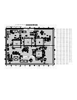
Страница 107: ...Circuit Diagrams and PWB Layouts EN 109 DVDR880 890 0X1 7 Layout Analog Board Top View TR 01045_001 150502 ...
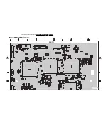
Страница 108: ...EN 110 DVDR880 890 0X1 7 Circuit Diagrams and PWB Layouts Layout Analog Board Overview Bottom View TR 01046_001 150502 ...
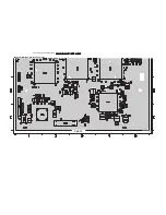
Страница 109: ...Circuit Diagrams and PWB Layouts EN 111 DVDR880 890 0X1 7 Layout Analog Board Part 1 Bottom View TR 01047_001 150502 ...
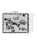
Страница 110: ...EN 112 DVDR880 890 0X1 7 Circuit Diagrams and PWB Layouts Layout Analog Board Part 2 Bottom View TR 01048_001 150502 ...
Страница 111: ...Circuit Diagrams and PWB Layouts EN 113 DVDR880 890 0X1 7 Test points overview Analog Board TR 01061_001 230502 ...
Страница 115: ...Circuit Diagrams and PWB Layouts EN 117 DVDR880 890 0X1 7 Tests points overview UPC12 Sub PCB TR 01053_001 140502 ...
Страница 165: ...Circuit IC Descriptions and List of Abbreviations EN 167 DVDR880 890 0X1 9 9 7 IC s Display Panel 9 7 1 IC7100 ...
Страница 166: ...Circuit IC Descriptions and List of Abbreviations EN 168 DVDR880 890 0X1 9 ...
Страница 167: ...Circuit IC Descriptions and List of Abbreviations EN 169 DVDR880 890 0X1 9 ...
Страница 174: ...Circuit IC Descriptions and List of Abbreviations EN 176 DVDR880 890 0X1 9 IC7411 ...
Страница 177: ...Circuit IC Descriptions and List of Abbreviations EN 179 DVDR880 890 0X1 9 9 9 IC sUPC12 Sub PCB 9 9 1 IC7825 ...
Страница 182: ...Circuit IC Descriptions and List of Abbreviations EN 184 DVDR880 890 0X1 9 ...
Страница 183: ...Circuit IC Descriptions and List of Abbreviations EN 185 DVDR880 890 0X1 9 ...
Страница 184: ...Circuit IC Descriptions and List of Abbreviations EN 186 DVDR880 890 0X1 9 ...
Страница 202: ...Circuit IC Descriptions and List of Abbreviations EN 204 DVDR880 890 0X1 9 9 11 IC s Divio Board 9 11 1 IC7404 NW700 ...
Страница 203: ...Circuit IC Descriptions and List of Abbreviations EN 205 DVDR880 890 0X1 9 ...

