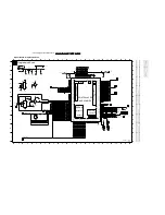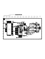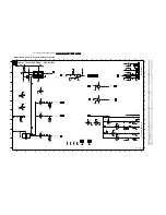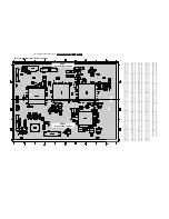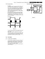
Circuit-, IC Descriptions and List of Abbreviations
EN 148
DVDR880-890 /0X1
9.
9.
Circuit-, IC Descriptions and List of Abbreviations
9.1
Display Board
9.1.1
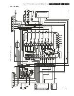
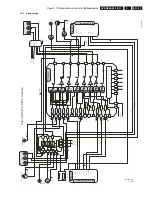
Microcontroller
The core element of the Display Control unit is the microcon-
troller TMP87CH74AF [7110]. The TMP87CH74AF is an 8 bit
microcontroller fitted with 32kB ROM and 1kB RAM. It requires
5V supply and is responsible for the following functions:
•
Interface to Central Controller-µP
•
Evaluation of the keyboard matrix
•
Decoding the remote control commands from the infra-red
receiver
•
Activation and control of the local display
•
Heater voltage generation
The 8 MHz resonator (Pos. 1111) generates the system clock.
The reset is generated by the CC-µP via “POR_DC”-signal
where the transistor [7106] is used as a level-shifter from 3V3
to 5V.
9.1.2
Interface to the Central Control
µ
P
The communication to the main microcontroller (CC) on the
µP-Sub-PCB is done via I
2
C-Interface, where the
TMP87CH74AF acts in slave-mode.
An additional wire (“INT”-line) is used to signal the Central
controller that data are ready, e.g. when a key has been
pressed.
9.1.3
Evaluation of the Keyboard Matrix
There are 10 different keys on the display board. A resistor
network is used to generate a specific direct voltage value,
depending on the pressed key. Via the resistors 3168 and
3169 on the analog/digital (A/D) ports (7110 pin 37 and 38) the
evaluation is done.
9.1.4
IR Receiver and Signal Evaluation
The IR receiver [7150] contains a selectively controlled ampli-
fier as well as a photo-diode. The photo-diode changes the
received infra red transmission (approx. 940nm) to electrical
pulses, which are then amplified and demodulated. On the
output of the IR receiver [7150], a pulse sequence with TTL-
level, which corresponds to the envelope curve of the received
IR remote control command, can be measured. This pulse
sequence is fed into the controller for further processing via
port TC1 [7110, pin20].
9.1.5
Vacuum Fluorescence Display
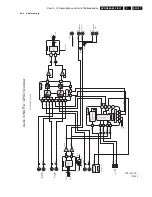
The VFD “10-BT-242GNK” [POS 7100] is fully controlled by
the microcontroller. The
µ
C also includes the driving stages.
Only two additional drivers [POS 7101 and 7102] are neces-
sary for the grids 8 and 10 because of their large size.
9.1.6
VFD Heater Voltage Generator
The circuit around POS [7103, 7104 and 7105] is used to gen-
erate a proper AC-Voltage for the filament of the VFD. For this
the microcontroller generates an appropriate rectangular sig-
nal with 50% duty-cycle and a frequency of 30 kHz at pin 19.
Pos. [5193] and [2102] are acting as a resonance-circuit. Via
Zener-Diode (POS[6100]) and resistors [3100, 3103 and
3104] the two heater-pins of the VFD (“FIL1” and “FIL2”) are
clamped so that the grids and segments can be fully switched
off.
9.1.7
REC-LED
The REC-LED is a red LED, located on a small PCB together
with the REC-Switch and controlled via pin 3 of the
microcontroller. The POS [7180] is used as a driver for the led.
9.2
Microcontroller Sub Board (UPC12 SUB PCB)
9.2.1
General
This small PCB is directly soldered in on top of the Analogue-
Board.
It is used with no diversity in all three different basic versions
(Europe, NAFTA and APAC-Pal). Only the software being
loaded into the external Flash-memory is not the same.
9.2.2
Microcontroller
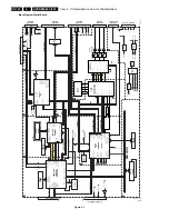
The main part of the Sub-PCB is the central controller (CC)
µ
P
[7804] TMP91CW12AF, which is a 16-bit CPU with
128kBROM and 4kB RAM.
It works with a 3V3 supply and a system clock of 24,576MHz
[1801].
The 3V3-supply is made out of the “5VSTBY” by the circuit
around [7816].
After connecting the set to the mains (power-up) the IC [7806]
generates a reset pulse. This signal (“IPOR”) is directly fed to
first priority interrupt input (pin 63) for power fail detection and
also to the Reset-Input of the CC (Pin30) via [7802], which is
necessary to generate a reset only during power-up. In case of
power fail pin 30 of the CC must be kept high (3V3).
The internal memory of the CC is too small for all necessary
demands. Therefore an external Flash-ROM [7805] with
1MByte in size and a RAM [7803] with 128kByte are neces-
sary. Both parts are connected to the
µ
P via a parallel
address-/data-bus. The lower eight bus-lines (AD0 to AD7) are
multiplexed by [7801] and the “ALE”-signal of the CC.
For updating of the software the external Flash-ROM can be
reprogrammed by the
µ
P. During this process [7807] is
switched on by the “WE”-signal.
When no mains is connected, the CC is supplied via Gold-Cap
[2816] during the power backup period. The diode [6802] pre-
vents unwanted current consumption of other components.
The internal ROM of the
µ
P holds the program code for the
Real-Time-Clock. Only the microprocessor is supplied by the
backup cell, not the external memories and the
µ
P operates in
a low frequency mode with the clock crystal [1805] only
(32.768 kHz). To adjust the clock the frequency can be mea-
sured at pin 87 of the
µ
P in a special test-mode.
9.2.3
Control-Interfaces
The CC is communicating with the digital board via a serial
connection, which operates at a speed of 19,4 kbit/s
(“D_DATA”-, “A_DATA”, “D_RDY”- and “A_RDY”-signal on
[1986]). By generating a high level on pin 16 of the CC the dig-
ital PCB can be reset (inverter [7817] in between).
Most of the other parts are controlled by the
µ
P via I
2
C-bus
(“SDA”- and “SCL”-signal). The FETs [7821] and [7822] are
used for adaptation of the 3V3-level on CC-side to the
components supplied with 5V.
The CC can also reset the display-board-
µ
P by pulling pin 39
to high.
The transistor [7819] acts as a level shifter for the “INT”-signal.
In the European sets a bi-directional interface is established
between the recording unit and the TV device at pin 10 of the
Scart (“P50”-line/Easy Link). The processing is done via pin 14
(output) and pin 38 (input) of the CC and the circuit around
[7813], [7814] and [7815].
Содержание DVDR880/001
Страница 45: ...Mechanical Instructions EN 47 DVDR880 890 0X1 4 4 2 Exploded View of the Set Figure 4 11 TR 01002_001 080502 ...
Страница 48: ...Mechanical Instructions EN 50 DVDR880 890 0X1 4 4 5 Dismantling Instructions Figure 4 14 ...
Страница 96: ...EN 98 DVDR880 890 0X1 7 Circuit Diagrams and PWB Layouts Layout Front Connector Panel FC TR 01030_001 150502 ...
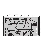
Страница 107: ...Circuit Diagrams and PWB Layouts EN 109 DVDR880 890 0X1 7 Layout Analog Board Top View TR 01045_001 150502 ...
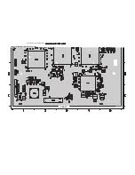
Страница 108: ...EN 110 DVDR880 890 0X1 7 Circuit Diagrams and PWB Layouts Layout Analog Board Overview Bottom View TR 01046_001 150502 ...
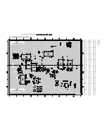
Страница 109: ...Circuit Diagrams and PWB Layouts EN 111 DVDR880 890 0X1 7 Layout Analog Board Part 1 Bottom View TR 01047_001 150502 ...
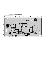
Страница 110: ...EN 112 DVDR880 890 0X1 7 Circuit Diagrams and PWB Layouts Layout Analog Board Part 2 Bottom View TR 01048_001 150502 ...
Страница 111: ...Circuit Diagrams and PWB Layouts EN 113 DVDR880 890 0X1 7 Test points overview Analog Board TR 01061_001 230502 ...
Страница 115: ...Circuit Diagrams and PWB Layouts EN 117 DVDR880 890 0X1 7 Tests points overview UPC12 Sub PCB TR 01053_001 140502 ...
Страница 165: ...Circuit IC Descriptions and List of Abbreviations EN 167 DVDR880 890 0X1 9 9 7 IC s Display Panel 9 7 1 IC7100 ...
Страница 166: ...Circuit IC Descriptions and List of Abbreviations EN 168 DVDR880 890 0X1 9 ...
Страница 167: ...Circuit IC Descriptions and List of Abbreviations EN 169 DVDR880 890 0X1 9 ...
Страница 174: ...Circuit IC Descriptions and List of Abbreviations EN 176 DVDR880 890 0X1 9 IC7411 ...
Страница 177: ...Circuit IC Descriptions and List of Abbreviations EN 179 DVDR880 890 0X1 9 9 9 IC sUPC12 Sub PCB 9 9 1 IC7825 ...
Страница 182: ...Circuit IC Descriptions and List of Abbreviations EN 184 DVDR880 890 0X1 9 ...
Страница 183: ...Circuit IC Descriptions and List of Abbreviations EN 185 DVDR880 890 0X1 9 ...
Страница 184: ...Circuit IC Descriptions and List of Abbreviations EN 186 DVDR880 890 0X1 9 ...
Страница 202: ...Circuit IC Descriptions and List of Abbreviations EN 204 DVDR880 890 0X1 9 9 11 IC s Divio Board 9 11 1 IC7404 NW700 ...
Страница 203: ...Circuit IC Descriptions and List of Abbreviations EN 205 DVDR880 890 0X1 9 ...

