Alignments
EN 146
DVDR880-890 /0X1
8.
8.2
Reprogramming Procedure of NVM on the
Microprocessor Sub PCB
The NVM, item 7808, on the Microprocessor Sub board
contains the following factory settings:
1.
Clock correction factor
2.
AFC reference value
3.
Slash version
The settings 1,2 and 3 are stored in the NVM during the
production of the analogue board.
The slash version is stored at the end of the production line of
the set.
In case of failure, the NVM must be replaced by an empty
device. By way of commands via the Diagnostic Software or via
ComPair, the factory settings must be restored in the NVM.
8.2.1
Clock Correction Adjustment
To guarantee an exact function of the real time clock, an
adjustment of the clock frequency is possibe. The adjustment
value is stored in the NVM.
Procedure:
•
put the set in service command mode
•
execute command 722 to initiate that a signal with 32768
Hz is available on pin 3 of connector 1988
DD:>722
•
measure the frequency f
meas
of the Clock Crystal with an
accuracy of ± 0.1 Hz.
•
Calculate the parameter to be entered: 32768/f
meas
* 10
6
•
Normally the parameter must be between 999902 and
1000097. If the parameter and therefore the frequency of
the crystal is outside this range, the crystal must be
replaced.
•
Execute command 721 with the parameter as input
example:
DD:>721 1000023
8.2.2
AFC Reference Voltage Tuner
This function stores the reference voltage for the tuner in the
NVM. Before this value can be stored, the AFC adjustment,
described in the adjustment instructions of the analogue board,
must be carried out.
Procedure:
•
Adjust AFC circuit
•
Calculate the reference value
•
Execute command 732 and use the calculated reference
value as parameter
example:
DD:>732 128
8.2.3
Slash Version
The slash version is stored with command 715 followed by the
slash version as parameter.
The slash versions used in DVDR880 and DVDR890 are the
following:
•
DVDR880/00X:
63
•
DVDR880/02X:
63
•
DVDR880/05X:
64
•
DVDR890/00X:
61
•
DVDR890/02X:
61
•
DVDR890/05X:
62
•
DVDR890/69X:
81
•
DVDR890/17X:
61
Example:
DD:>715 63
Reset of Slash Version
Use command 729 to reset the analogue board to the default
setting.
Procedure:
•
Put the set in DSW command mode
•
Execute command 729 with the following parameters:
DD:> 729 w 0xA0 3 0x07 0xD0 0x00
•
Leave the DSW command mode and start up the set in
application mode
No background is visible on the TV screen. The analogue
board is ready to accept the appropriate slash version
8.3
Rework Procedure IEEE Unique Number
8.3.1
Scope:
The procedure describes how to upgrade sets with a unique
number after repair. This unique number is stored in the
NVRAM (item 7201) of the digital board at the end of the
production line.
This procedure is only valid or necessary when:
•
The digital board is replaced
•
NVRAM on the digital board is replaced
•
NVRAM is cleared
In all other cases the repaired set retains its unique number.
The procedure defines several means to re-assure the unique
number depending on the possibilities of repair or the state the
faulty set is in.
8.3.2
Handling:
State of original (defective) board:
1.
The digital board starts up in Diagnostics Mode: follow
procedure A to retrieve the valid unique number
2.
The digital board does NOT start up in Diagnostics Mode:
follow procedure B.
8.3.3
Procedure A
1.
Connect defective digital board to PC via serial cable (3122
785 90017)
2.
start up hyper terminal or any other serial terminal via the
correct settings (DSW command mode interface)
3.
read out existing unique number via nucleus 403
example:
DD:> 403
40300: DV Unique ID = 00D7A1FC6C
Test OK @
4.
note read out
5.
program new digital board via nucleus 410
example: DD:> 410 00D7A1FC6C
41000:
Test OK @
The set has now the original unique number
Содержание DVDR880/001
Страница 45: ...Mechanical Instructions EN 47 DVDR880 890 0X1 4 4 2 Exploded View of the Set Figure 4 11 TR 01002_001 080502 ...
Страница 48: ...Mechanical Instructions EN 50 DVDR880 890 0X1 4 4 5 Dismantling Instructions Figure 4 14 ...
Страница 96: ...EN 98 DVDR880 890 0X1 7 Circuit Diagrams and PWB Layouts Layout Front Connector Panel FC TR 01030_001 150502 ...
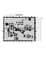
Страница 107: ...Circuit Diagrams and PWB Layouts EN 109 DVDR880 890 0X1 7 Layout Analog Board Top View TR 01045_001 150502 ...
Страница 108: ...EN 110 DVDR880 890 0X1 7 Circuit Diagrams and PWB Layouts Layout Analog Board Overview Bottom View TR 01046_001 150502 ...
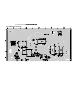
Страница 109: ...Circuit Diagrams and PWB Layouts EN 111 DVDR880 890 0X1 7 Layout Analog Board Part 1 Bottom View TR 01047_001 150502 ...
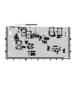
Страница 110: ...EN 112 DVDR880 890 0X1 7 Circuit Diagrams and PWB Layouts Layout Analog Board Part 2 Bottom View TR 01048_001 150502 ...
Страница 111: ...Circuit Diagrams and PWB Layouts EN 113 DVDR880 890 0X1 7 Test points overview Analog Board TR 01061_001 230502 ...
Страница 115: ...Circuit Diagrams and PWB Layouts EN 117 DVDR880 890 0X1 7 Tests points overview UPC12 Sub PCB TR 01053_001 140502 ...
Страница 165: ...Circuit IC Descriptions and List of Abbreviations EN 167 DVDR880 890 0X1 9 9 7 IC s Display Panel 9 7 1 IC7100 ...
Страница 166: ...Circuit IC Descriptions and List of Abbreviations EN 168 DVDR880 890 0X1 9 ...
Страница 167: ...Circuit IC Descriptions and List of Abbreviations EN 169 DVDR880 890 0X1 9 ...
Страница 174: ...Circuit IC Descriptions and List of Abbreviations EN 176 DVDR880 890 0X1 9 IC7411 ...
Страница 177: ...Circuit IC Descriptions and List of Abbreviations EN 179 DVDR880 890 0X1 9 9 9 IC sUPC12 Sub PCB 9 9 1 IC7825 ...
Страница 182: ...Circuit IC Descriptions and List of Abbreviations EN 184 DVDR880 890 0X1 9 ...
Страница 183: ...Circuit IC Descriptions and List of Abbreviations EN 185 DVDR880 890 0X1 9 ...
Страница 184: ...Circuit IC Descriptions and List of Abbreviations EN 186 DVDR880 890 0X1 9 ...
Страница 202: ...Circuit IC Descriptions and List of Abbreviations EN 204 DVDR880 890 0X1 9 9 11 IC s Divio Board 9 11 1 IC7404 NW700 ...
Страница 203: ...Circuit IC Descriptions and List of Abbreviations EN 205 DVDR880 890 0X1 9 ...

