MS51
Dec. 17, 2019
Page
284
of 316
Rev 1.01
M
S51
SE
RIES
TE
CHNICA
L REF
ERE
N
CE MA
NU
A
L
16-bit
up/down
counter
PWMn_CH0
PWMn_CH1
PWMn_CH2
Pre-scalar
INTSEL[1:0], INTTYP[1:0]
(PWMnCON0[3:0])
PWMRUN
(PWMnCON0.7)
CLRPWM
(PWMnCON0.4)
PWMP
registers
LOAD (PWMnCON0.6)
PWMF
(PWMnCON0.5)
PWMP buffer
PWM0 buffer
PWM0 Register
0-to-1
PWM and
Fault Brake
output
control
PWMTYP
(PWMnCON1.4)
edge/center
Interrupt
select/type
PWMDIV0[2:0]
(PWMnCON1[2:0])
PG0
PWM interrupt
Brake event
(PWM_BRAKEn)
0
1
Timer 1 overflow
PWMCKS
(CKCON.6)
F
PWM
=
Counter
Matching(edgealigned)/
underflow(venter aligned)
F
SYS
clear counter
=
PWM1 buffer
PWM1 Register
PG1
=
PWM2 buffer
PWM2 Register
=
PWM3 buffer
PWM3 Register
=
PWM4 buffer
PWM4 Register
=
PWM5 buffer
PWM5 Register
=
PG2
PG3
PG4
PG5
0
1
0
1
0
1
0
1
GP
[PWMnCON1.5]
(PWMnPH,
PWMnPL)
(PWMnCH0H,
PWMnCH0L)
(PWMnCH1H,
PWMnCH1L)
(PWMnCH2H,
PWMnCH2L)
(PWMnCH3H,
PWMnCH3L)
(PWMnCH4H,
PWMnCH4L)
(PWMnCH5H,
PWMnCH5L)
PWMn_CH3
PWMn_CH4
PWMn_CH5
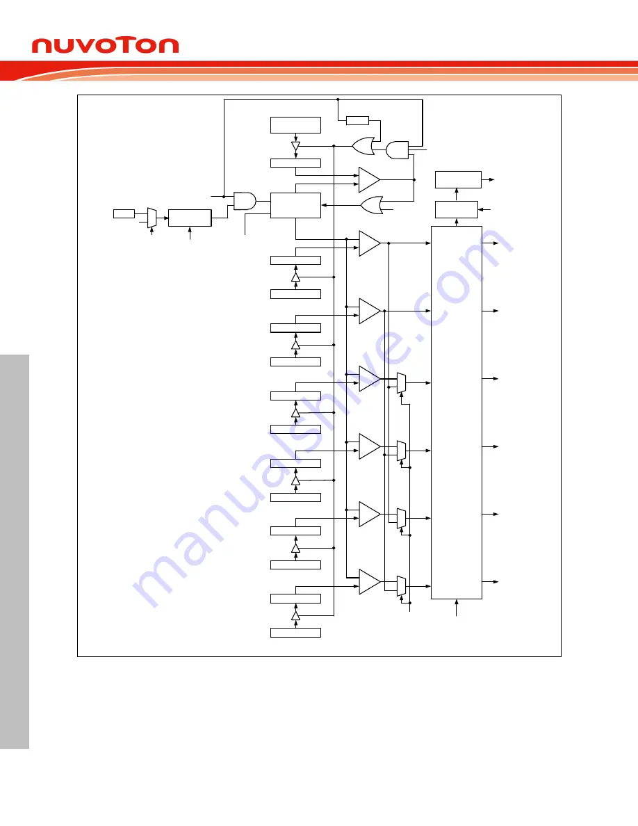
Figure 6.11-1 PWM Block Diagram
The PWM counter generates six PWM signals called PG0, PG1, PG2, PG3, PG4, and PG5. These
signals will go through the PWM and Fault Brake output control circuit. It generates real PWM outputs
on I/O pins. The output control circuit determines the PWM mode, dead-time insertion, mask output,
Fault Brake control, and PWM polarity. The last stage is a multiplexer of PWM output or I/O function.


