M68360QUADS-040 Hardware User’s Manual
GENERAL INFORMATION
9
1.6
FEATURES
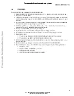
Following are the main features of the M68360QUADS-040:
❏
Master MC68EC040FE33 with 32-bit address bus, 32 bit data bus, instruction and data caches.
❏
Supports also MC68LC040.
❏
1 Mbyte Dynamic RAM, 60 nsec access time, 36 bits wide (data and parity) SIMM, accessed with
3,2,2,2 clock cycles. Support for dram SIMMs upto 8 Mbyte with automatic size and speed
detection.
❏
512 Kbyte Flash PROM, On-board (5V) programmable, individual sector protection, 32 bits wide,
120 nsec access time, support is given up to 2 Mbyte.
❏
128K byte synchronous bursting sram, 36 bits wide, 12 nsec access time. Accessed with 3,1,1,1
clock cycles. Option for additional 128K Byte identical bank.
❏
256 byte serial EEPROM, accessed by the SPI port.
❏
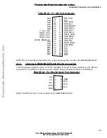
Application Development Interface (ADI) port via 37 pin D-type connector.
❏
Serial RS-232 port for terminal or host computer connection via 9 pin Dtype connector.
❏
Two
Ethernet ports:
1.
The first using Motorola’s MC68160 (EEST) with both AUI and TP connectors.
2.
The second using AMD’s Am7992 (SIA) with AUI connector.
❏
SCC2 (connected to the second Ethernet port) may be used for other purpose, by removing the
SIA from its socket.
❏
Expansion and Logic Analyzer connectors for both slave QUICC and MC68EC040.
❏
Slave QUICC (core disabled in 68EC040 companion mode) providing the following functions:
1.
DRAM Controller
2.
Chip Select, TA~ and DSACK~ generator.
3.
Parallel port (ADI) controller.
4.
UART for terminal or host computer connection.
F
re
e
sc
a
le
S
e
m
ic
o
n
d
u
c
to
r,
I
Freescale Semiconductor, Inc.
For More Information On This Product,
Go to: www.freescale.com
n
c
.
..


