M68360QUADS-040 Hardware User’s Manual
Hardware Preparation and Installation
14
2.3.2
Caches Enable / Disable
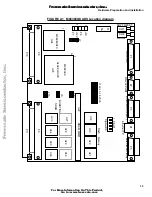
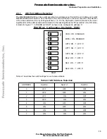
Switch #1 on DSW1 enables / disables the MC68EC040 caches. When it is in ’OFF’ position (FACTORY
SETUP) both caches may be enabled by software. When it is in ’ON’ position, both instruction and data
caches can not be enabled by software.
2.3.3
MMU Enable / Disable
Switch #2 on DSW1 enables / disables the Memory Management Unit, which exists only on a MC68LC040
processor. When a MC68EC040 is installed, this switch has no effect. When switch #2 is in ’OFF’ position
the MMU (if exists) is enabled, when in ’ON’ position - the MMU (if exists) is disabled.
Hardware Break Point Logic Configuration
The Hardware BreakPoint Out signal (BKPTO~) of the QUICC may be used for 2 purposes:
1.
Generating level 7 interrupt (NMI) to the EC040, serving its original purpose.
2.
A caching shield logic, to avoid redundant caching of data into the data cache
The selection between the above is done via jumper J7. When pins 1 and 2 of J7 are connected, the
breakpoint logic functions in its original goal. When pins 2 and 3 of J7 are connected, the breakpoint logic
serves a data caching shield.
J7 is configured at factory to position 1-2.
2.3.4
Parity Error Interrupt Generation
When the QUICC’s parity logic is operating, i.e., parity is generated and checked by the memory controller,
it is possible to generate level 5 interrupt to the EC040 when parity error is encountered. When jumper J8
is connected, the QUICC’s Parity Error line (PERR~) is connected to the QUICC’s level 5 interrupt request
line - IRQ5~ to generate level 5 interrupt upon parity error occurrence. When J8 is disconnected, no parity
error interrupt is generated.
J8 is disconnected at factory.
2.3.5
Arbitration Configuration
To allow for external master to be connected off-board, the arbitration scheme must be changed.
Jumper J9 connects between the EC040 Bus Request Output (BR040~) and QUICC’s Bus Request Input
(BRQ~), while J10 connects between the QUICC’s Bus Grant Output (BGQ~) and the EC040’s Bus Grant
Input (BG040~). When BOTH J9 and J10 are connected, arbitration is done by the QUICC’s arbiter. When
BOTH J9 and J10 are DISCONNECTED, an external arbiter may be introduced via the expansion
connectors.
BOTH J9 & J10 are connected at factory.
2.3.6
EEST Configuration
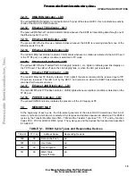
The configuration of the MC68160 - EEST is determined by the position of jumpers J1 to J6. For the
concise description of the role of each jumper see section 3.2.4 on page 17. The EEST is factory set to AUI
interface, i.e., jumpers J1, J2 & J6 connected and J2 - J5 disconnected.
2.3.7
User Selectable Options
Since the state of switches #3 to #5 is readable to software via the board status-register, it is possible to
use them for software configuration, modes’ selection, etc. For further information on that subject see
4.11.5 on page 35.
2.4
INSTALLATION INSTRUCTIONS
When the M68360QUADS-040 has been configured as desired by the user, it can be installed according
to the required working environment as follows:
F
re
e
sc
a
le
S
e
m
ic
o
n
d
u
c
to
r,
I
Freescale Semiconductor, Inc.
For More Information On This Product,
Go to: www.freescale.com
n
c
.
..


