


2-21
AC Timings
Note:
The timing values listed are preliminary and refer to minimum system timing requirements.
Actual implementation requires conformance to the specific protocol requirements. Refer to
Chapter 1 to identify the specific input and output signals associated with the referenced
internal controllers and supported communication protocols. For example, FCC1 supports
ATM/Utopia operation in slave mode, multi-PHY master direct polling mode, and multi-PHY
master multiplexed polling mode and each of these modes supports its own set of signals; the
direction (input or output) of some of the shared signal names depends on the selected mode.
2.7.6 EE Signals
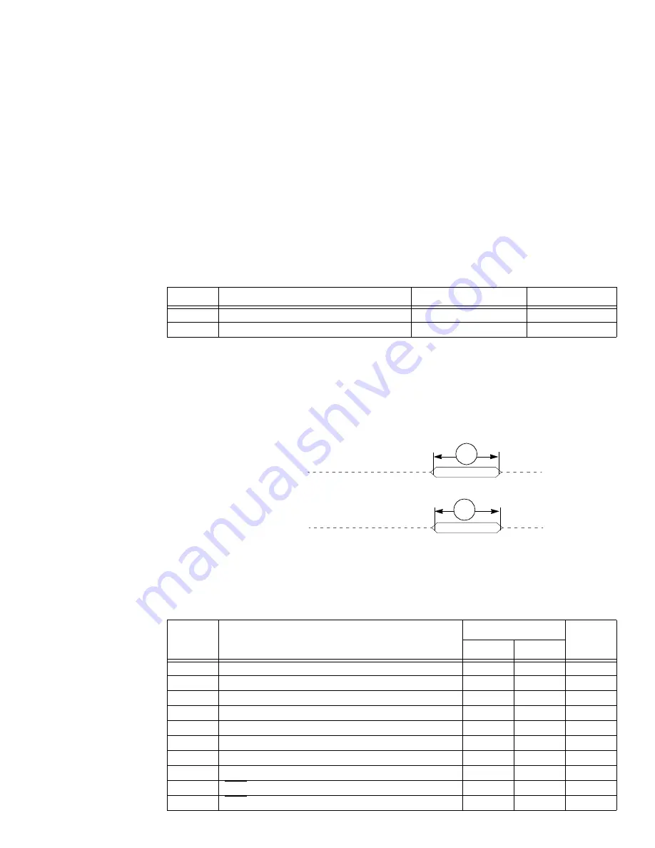
Figure 2-20 shows the signal behavior of the
EE
pins.
2.7.7 JTAG Signals
Table 2-21. EE Pins Timing
Number
Characteristics Type
Minimum
65
EE pins as inputs
Asynchronous
4 DSPCLKs
66
EE pins as outputs
Synchronous to DSPCLK
1 DSPCLK
Notes:
1.
DSPCLK is the SC140 core clock. The ratio between DSPCLK and CLKOUT is configured during
power-on-reset. See AN2288 for details.
2.
Direction of the EE pins is configured in the EE_CTRL register of the EOnCE (See the
SC140 Core
Reference Manual
, MNSC140DSPCORERM/D).
3.
Refer to Table 1-3 on page 1-6 for detailed information about EE pin functionality.
Figure 2-20. EE Pins Timing
Table 2-22. JTAG Timing
No.
Characteristics
All frequencies
Unit
Min Max
500
TCK frequency of operation
0.0
40.0
MHz
501
TCK cycle time
25.0
—
ns
502
TCK clock pulse width measured at 1.6 V
12.5
—
ns
503
TCK rise and fall times
0.0
3.0
ns
508
TMS, TDI data set-up time
6.0
—
ns
509
TMS, TDI data hold time
3.0
—
ns
510
TCK low to TDO data valid
0.0
5.0
ns
511
TCK low to TDO high impedance
0.0
5.0
ns
512
TRST assert time
100.0
—
ns
513
TRST set-up time to TCK low
40.0
—
ns
EEi, EED out
EEi, EED in
65
66


