


1-17
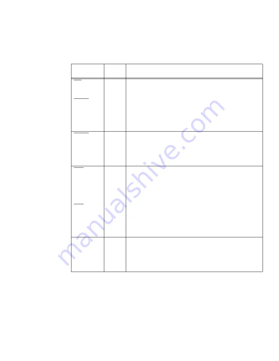
Memory Controller Signals
POE
PSDRAS
PGPL2
Output
Output
Output
Bus Output Enable
Output of the bus GPCM. Controls the output buffer of memory devices during read
operations.
Bus SDRAM RAS
Output from the bus SDRAM controller. This pin should connect to the SDRAM
Row Address Strobe (RAS) input signal.
Bus UPM General-Purpose Line 2
One of six general-purpose output lines from the UPM. The values and timing of
this pin are programmed in the UPM.
PSDCAS
PGPL3
Output
Output
Bus SDRAM CAS
Output from the bus SDRAM controller. This pin should connect to the SDRAM
Column Address Strobe (CAS) input signal.
Bus UPM General-Purpose Line 3
One of six general-purpose output lines from the UPM. The values and timing of
this pin are programmed in the UPM.
PGTA
PUPMWAIT
PPBS
PGPL4
Input
Input
Output
Output
GPCM TA
Terminates transactions during GPCM operation. Requires an external pull up
resistor for proper operation.
Bus UPM Wait
Input to the UPM. An external device can hold this pin high to force the UPM to wait
until the device is ready for the operation to continue.
Bus Parity Byte Select
In systems in which data parity is stored in a separate chip, this output is the
byte-select for that chip.
Bus UPM General-Purpose Line 4
One of six general-purpose output lines from the UPM. The values and timing of
this pin are programmed in the UPM.
PSDAMUX
PGPL5
Output
Output
Bus SDRAM Address Multiplexer
Controls the SDRAM address multiplexer when the MSC8101 is in External Master
mode.
Bus UPM General-Purpose Line 5
One of six general-purpose output lines from the UPM. The values and timing of
this pin are programmed in the UPM.
Table 1-2. Memory Controller Signals (Continued)
Signal
Data
Flow
Description


