


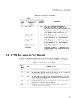

1-30
Communications Processor Module (CPM) Ports
PB22
FCC2: TXD0
MII
and
HDLC nibble
FCC2: TXD
HDLC serial
and
transparent
SI1 TDMA1: L1RXD1
TDM nibble
SI2 TDMD2: L1RXD
TDM serial
Output
Output
Input
Input
FCC2: MII and HDLC Nibble Transmit Data Bit 0
TXD[0–3] is supported by MII and HDLC nibble mode in
FCC2. TXD3 is the most significant bit. TXD0 is the least
significant bit.
FCC2: HDLC Serial and Transparent Transmit Data
TXD is supported by HDLC serial mode and transparent
mode in FCC2.
Time-Division Multiplexing A1: Nibble Layer 1 Receive
Data Bit 1
In the TDMA1 interface supported by SI1. TDMA1 supports
bit and nibble modes. L1RXD3 is the most significant bit.
L1RXD0 is the least significant bit in nibble mode. TDMA1
receives nibble data from L1RXD[0–3].
Time-Division Multiplexing D2: Layer 1 Receive Data
In the TDMD2 interface supported by SI2. TDMD2 supports
serial mode. TDMD2 receives serial data from L1RXD.
PB21
FCC2: RXD0
MII
and
HDLC nibble
FCC2: RXD
HDLC serial
and
transparent
SI1 TDMA1: L1TXD2
TDM nibble
SI2 TDMD2: L1TSYNC
TDM serial
Input
Input
Output
Input
FCC2: MII and HDLC Nibble Receive Data Bit 0
RXD[0–3] is supported by MII and HDLC nibble mode in
FCC2. RXD3 is the most significant bit. RXD0 is the least
significant bit.
FCC2: HDLC Serial and Transparent Receive Data
Supported by HDLC serial mode and transparent mode in
FCC2.
Time-Division Multiplexing A1: Nibble Layer 1 Transmit
Data Bit 2
In the TDMA1 interface supported by SI1. TDMA1 supports
bit and nibble modes. L1TXD3 is the most significant bit.
L1TXD0 is the least significant bit in nibble mode. TDMA1
transmits nibble data out of L1TXD[0–3].
Time-Division Multiplexing D2: Layer 1 Transmit
Synchronize Data
In the TDMD2 interface supported by SI2, this is the
synchronizing signal for the transmit channel. See the
Serial
Interface with Time-Slot Assigner
chapter in the
MSC8101
Technical Reference
manual.
Table 1-4. Port B Signals (Continued)
Name
Dedicated
I/O Data
Direction
Description
General-
Purpose
I/O
Peripheral Controller:
Dedicated I/O
Protocol


