


4-4
Layout Practices
4.4 Layout Practices
Each
V
CC
and
V
DD
pin on the MSC8101 should be provided with a low-impedance path to the board’s
power supply. Similarly, each
GND
pin should be provided with a low-impedance path to ground. The
power supply pins drive distinct groups of logic on the chip. The
V
CC
power supply should be bypassed
to ground using at least four 0.1 µF by-pass capacitors located as closely as possible to the four sides of
the package. The capacitor leads and associated printed circuit traces connecting to chip
V
CC
,
V
DD
, and
GND
should be kept to less than half an inch per capacitor lead. A four-layer board is recommended,
employing two inner layers as
V
CC
and
GND
planes.
All output pins on the MSC8101 have fast rise and fall times. Printed circuit board (PCB) trace
interconnection length should be minimized in order to minimize undershoot and reflections caused by
these fast output switching times. This recommendation particularly applies to the address and data
busses. Maximum PCB trace lengths of six inches are recommended. Capacitance calculations should
consider all device loads as well as parasitic capacitances due to the PCB traces. Attention to proper PCB
layout and bypassing becomes especially critical in systems with higher capacitive loads because these
loads create higher transient currents in the
V
CC
,
V
DD
, and
GND
circuits. Pull up all unused inputs or
signals that will be inputs during reset. Special care should be taken to minimize the noise levels on the
PLL supply pins.
There are 2 pairs of PLL supply pins:
V
CCSYN
-
GND
SYN
and
V
CCSYN1
-
GND
SYN1
. Each pair supplies one
PLL. To ensure internal clock stability, filter the power to the
V
CCSYN
and
V
CCSYN1
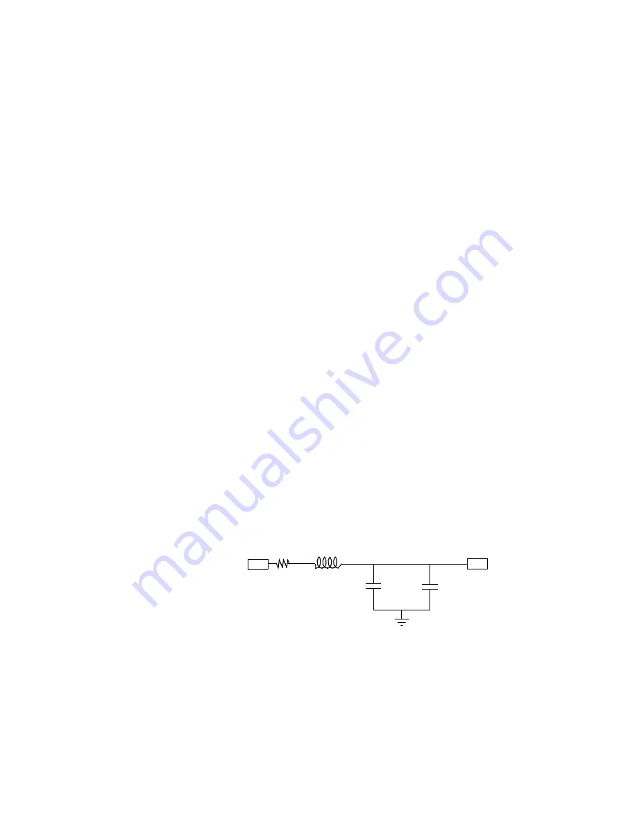
inputs with a circuit
similar to the one in Figure 4-2.. To filter as much noise as possible, place the circuit as close as possible
to
V
CCSYN
and
V
CCSYN1
. The 0.01-µF capacitor should be closest to
V
CCSYN
and
V
CCSYN1
, followed by
the 10-µF capacitor, the 10-nH inductor, and finally the 10-
Ω
resistor to
V
DD
. These traces should be kept
short and direct.
GND
SYN
and
GND
SYN1
should be provided with an extremely low impedance path to ground and should
be bypassed to
V
CCSYN
and
V
CCSYN1
, respectively, by a 0.01-µF capacitor located as close as possible to
the chip package. The user should also bypass
GND
SYN
and
GND
SYN1
to
V
CCSYN
and
V
CCSYN1
with a
0.01-µF capacitor as closely as possible to the chip package
Figure 4-2. VCCSYN and VCCSYN1 Bypass
V
DD
0.01 µF
10 µF
V
CCSYN
10
Ω
10nH