background image

CPU Interface Design Considerations

Layout Instructions

Copyright © 2002 Marvell

CONFIDENTIAL

Doc. No. MV-S300165-00, Rev. A

May 21, 2002, Preliminary

Document Classification: Proprietary Information

 Page 105


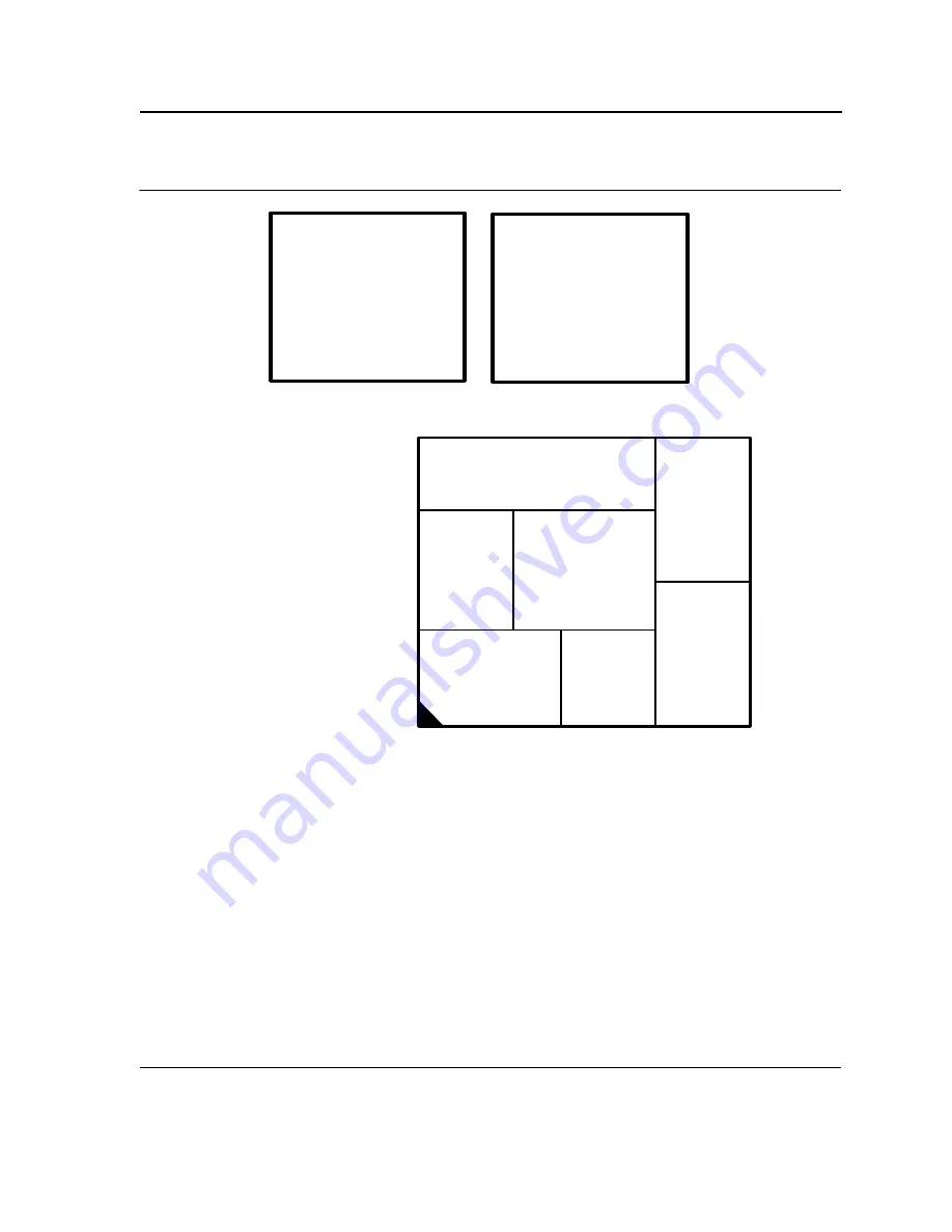
Figure 57: Layout for a Single GT-64260A to Multiple CPUs     

The placement for multi-GT mode depends on the number of GT-64260A devices and interfaces used on each one 
of them.

Depending on the system configuration and timing simulation, parallel termination on the bi-directional signals can 
be placed near the CPUs or the GT-64260As.

14.5.2 Routing

The CPU interface traces must be 55 to 65 Ohm impedance.

The CPU and GT-64260A clocks (see section 

Section 19. "Clocks" on page 143

) must be routed on separate lay-

ers from the other signals.

The point-to-multipoint topology signals must be routed in a "V" or "T" shape.

GT-64260A

CPU interface

PCI0

PCI1

SDRAM

Comm.

Device

A B C D . . .

.
.
.
4
3
2
1

CPU0

CPU1

Содержание GT-64260A

Страница 1: ...GT 64260A Design Guide Doc No MV S300165 00 Rev A May 21 2002 ...

Страница 2: ...rticular optional function Should the user choose to implement any of these optional functions it is possible that the use could be subject to third party intellectual property rights Marvell recommends that the user investigate whether third party intellectual property rights are relevant to the intended use of these products and obtain licenses as appropriate under relevant intellectual property...

Страница 3: ... 18 3 4 Cache Coherency 18 3 5 Specific CPUs Aspects 21 3 6 Multi GT or Multi slave Modes 24 3 7 CPU Bus Multiple Masters 26 3 8 PowerPC COP JTG Interface 31 SECTION 4 SDRAM INTERFACE FUNCTIONAL OVERVIEW 33 4 1 Pinout Description 33 4 2 Memory Connection 35 4 3 SDRAM Address Control 39 4 4 SDRAM Initialization 40 4 5 ECC Support 40 4 6 Memory Banks and Pages 42 SECTION 5 PCI INTERFACE FUNCTIONAL O...

Страница 4: ...urst SRAM 60 SECTION 7 COMMUNICATION INTERFACE FUNCTIONAL OVERVIEW 61 7 1 Ethernet Controllers 61 7 2 MPSC Controllers 62 7 3 Cache Coherency 62 7 4 MPSC and Ethernet SW Implications 63 7 5 I2C Interface 70 7 6 Baud Rate Generator 72 SECTION 8 MULTI PURPOSE PIN INTERFACE FUNCTIONAL OVERVIEW 74 8 1 General Purpose Pin GPP 74 8 2 Interrupt Outputs 75 8 3 PCI Arbiter 76 8 4 DMA Request 76 8 5 DMA ack...

Страница 5: ... 12 1 Messaging 87 12 2 Doorbell 87 12 3 Circular Queue 88 SECTION 13 DESIGN CONSIDERATION OVERVIEW 90 SECTION 14 CPU INTERFACE DESIGN CONSIDERATIONS 91 14 1 CPU Interface Connectivity 91 14 2 Electrical Specification 92 14 3 Termination Topology 92 14 4 Timing Requirements 92 14 5 Layout Instructions 104 SECTION 15 SDRAM INTERFACE DESIGN CONSIDERATIONS 106 15 1 Interface Connectivity 106 15 2 Ele...

Страница 6: ...tion Topology 135 17 4 Timing Requirements 135 17 5 Layout Instructions 138 SECTION 18 POWER SUPPLY 140 18 1 De coupling Recommendations 140 SECTION 19 CLOCKS 143 SECTION 20 RESET 144 20 1 Reset Configurations 144 SECTION 21 BRINGING UP THE SYSTEM DEBUGGING 145 21 1 Communication Unit 145 SECTION 22 REVISION HISTORY 146 APPENDIX A I2C EEPROM EXAMPLE 147 APPENDIX B SDRAM MODE REGISTER CODE 149 APPE...

Страница 7: ...0165 00 Rev A May 21 2002 Preliminary Document Classification Proprietary Information Page 7 D 3 PCI Interface 153 D 4 Swapping Options 153 APPENDIX E COMMUNICATION EXAMPLE CODE 158 E 1 Ethernet Initialization 158 E 2 Ethernet API 159 E 3 MPSC API 160 ...

Страница 8: ...iming 98 Table 17 Multiple GT 64260As and a Single CPU AC Timing 101 Table 18 Signal Topology Categories 109 Table 19 Trace Length for Data Topologies 114 Table 20 GT 64260A SDRAM Interface AC Timing 115 Table 21 Typical SDRAM Interface AC Timing 115 Table 23 GT 64260A CS AC Timing 121 Table 24 Typical SDRAM CS AC Timing 121 Table 22 Trace Length for Data Topologies 121 Table 25 Trace Length for D...

Страница 9: ...re 17 Single Read Access to Open Page 44 Figure 18 Typical P2P System Configuration 46 Figure 19 I O P2P Transaction Example 47 Figure 20 Three Device Connection Example 52 Figure 21 8 bit Device Connection Example 54 Figure 22 16 bit Device Connection Example 55 Figure 23 32 bit Device Connection Example 57 Figure 24 Device Burst Read Example 58 Figure 25 Device Burst Write Example 59 Figure 26 S...

Страница 10: ...imulation Example With Resistors 109 Figure 62 DIMM Clock Topology 111 Figure 63 GT 64260A Data Reference Point 112 Figure 64 SDRAM Data Reference Point 113 Figure 65 Selected Memory Configuration Data Topology 114 Figure 66 DIMM Connector Package Model 115 Figure 67 0 8 ns Delay Trace Simulation 2 1 ns Fly Time Reference Point 116 Figure 68 0 8 ns Delay Trace Simulation 1 54 ns Fly Time Reference...

Страница 11: ...tation The following documents are referenced by this design guide or provide additional information about working with the GT 64260A See the Marvell website at http www marvell com to access this material GT 64260A Datasheet Doc No MV S100413 00 EV 64260A BP xxxxx Reference Platform Schematics PCI 2 2 Local Bus Specification AN 66 Initializing Ethernet Ports AN 67 Powering Up Powering Down Galile...

Страница 12: ...bps Ethernet ports and two MPSC controllers The GT 64260A provides a single chip solution for designers building systems for a PowerPC 64 bit bus CPU It has the following interfaces A 64 bit interface to the CPU bus A 64 bit interface to SDRAM A 32 bit interface to devices various types of memory and I O devices Two 64 bit PCI interfaces Three RMII MII interfaces Two MPSC communication interfaces ...

Страница 13: ...inary Document Classification Proprietary Information Page 13 Figure 2 Typical GT 64260A System Configuration PowerPC CPU 2 Gigabyte DRAM Routing Unit 8xIDMA 3x10 100 2xMPSC GPP SDRAM i f Device i f CPU I f PCI0 i f Boot Flash OC 48 Framing ASIC Box Mang Bus UART Monitor Back Plane Tranceiver PCI0 i f ...

Страница 14: ...ces such as SDRAM ROM PCI etc Generally there is a point to point connection between the GT 64260A and the CPU In other cases it depends on the system architecture such as multi GT 64260A multiple CPU or exter nal arbiter The following table describes the pin information and details of the GT 64260A CPU interface Table 1 CPU Interface Pin Information Pin Name Input Output PowerPC CPU Pin Connectio...

Страница 15: ...10K Ohm Pull up Address tenure start TSIZ 0 2 T S I O TSIZ 0 2 10K Ohm Pull up Transfer size TBST T S I O TBST 10K Ohm Pull up Transfer burst TT 0 4 T S I O TT 0 4 10K Ohm Pull up Transfer type TA T S I O TA In multi GT mode requires 10K Ohm Pull up Transfer acknowledge AACK T S I O AACK In multi GT mode requires 10K Ohm Pull up Address acknowledge ARTRY T S I ARTRY 10K Ohm Pull up Address retry N...

Страница 16: ...her configu rations 10K Ohm pull down Data transfer index BR0 GT_BG I When using the GT 64260A internal arbiter connect to the primary CPU BR pin When using an external arbiter connect to the arbiter GT_BG pin NOTE In single CPU systems with the internal arbiter enabled must be used as BR0 To avoid unstable states at reset a 10K Ohm Pull up is recommended BG0 T S O When using the GT 64260A interna...

Страница 17: ...er is used a 10K Ohm Pull up is recommended BR1 GT_DBG I When using single CPU sys tems this pin can be left as not connected NC When using the GT 64260A internal arbiter connect to the secondary CPU BR pin When using an external arbiter connect to the arbiter GT_DBG pin To avoid unstable states at reset or in a single CPU configu ration a 10K Ohm Pull up is recom mended DBG1 T S O When using an e...

Страница 18: ...caches Any access to the SDRAM from PCI or IDMA may result in a snoop transaction driven by the GT 64260A on the CPU bus The SDRAM access to a cache coherent region is always suspended until the snoop is resolved In case of a HIT in a modified line in CPU cache the SDRAM access might be suspended until the line write back to SDRAM is completed Figure 3 describes the transaction flow for PCI reads ...

Страница 19: ...action address is compared against the four cache coherency regions If an address hits one of these regions the DRAM access results in a snoop action based on cache pol icy WB WT as defined by the snoop regions registers Additionally the CPU Master Control register s CleanBlock and FlushBlock bits 13 12 at offset 0x160 must be set to the appropriate value depending on the CPU type Table 3 IDMA Add...

Страница 20: ... tion for more information 3 Configure cache coherent windows for the desired interface with the PCI cache coherency registers 0x1F00 0x1F38 and the IDMA cache coherency registers 0x380 0x3B8 4 Confirm that the Snoop Control Base Low register s Snoop bits 13 12 at offset 0x1F00 0x1F30 are set to the correct value depends on the CPU cache policy WB or WT NOTE The cache coherency will not be enabled...

Страница 21: ... bit device e g SRAM For example the GT 64260A with the MPC745x evaluation platform EV 64260ABP MPC7450 uses an 8 bit wide flash device and a 32 bits wide SRAM device to boot the CPU Before the CPU reset de assertion the 8 bit flash is copied to the 32 bits SRAM device by the I2C interface Note For more information on the serial ROM initialization see the GT 64260A datasheet s Reset Configuration ...

Страница 22: ...et even when the serial ROM is enabled This means the CPU interface voltage value AD 31 and the serial initialization value AD 0 must be the same 3 5 3 MPC745x Extended Pins The MPC745x CPU supports a 32 bit addressing mode and a 36 bit extended addressing modes When extended physical addressing is disabled the MPC745x drives the four most significant bits to zeroes Note The four most significant ...

Страница 23: ...e the IOs one way or the other any control signals that must be in a par ticular state leaving HRESET have to be either driven to that state or pulled there by external resistors The designer can connect two keepers on the same signals i e multiple PPC750FX systems since they will always drive the same value Theoretically two keepers can end up in contention during power up However since this woul...

Страница 24: ...als low and the signal voltage reaches the GND value Note For more information see the IBM datasheet 3 5 5 PPC750FX Data Bus Parking The GT 64260A internal 60x arbiter supports data bus parking See the GT 64260A errata and restriction document errata FEr CPU 1 Multiple data bus masters with IBM PPC750CX e CPUs This errata is also applicable to PPC750FX DD1 x Revisions The dd2 0 Revision and higher...

Страница 25: ...ices must be tied together to drive the CPU AACK input When multi GT is enabled after reset de assertion the GT 64260A uses a reduced address decoding scheme as long as the CPU Configuration register s MultiGTDec bit 18 at offset 0x000 is set to 1 In this mode each GT 64260A device has a two bit ID that is sampled at reset on AD 11 10 pins Each device responds to the transac tion address that matc...

Страница 26: ...sses The arbitration must be implemented to support multiple masters on the CPU bus The multiple masters configuration is usually used in a Symmetric Multiple Processing SMP system For an SMP system to be fully functional it requires additional HW implementations 3 7 1 PowerPC Bus Arbitration The GT 64260A supports both external arbiter and internal arbiter configurations The arbiter configuration...

Страница 27: ...t first To enable CPU1 to access the bus set the CPU Master Control register s MaskBR1 bit 9 at offset 0x160 to 0 If the internal arbiter is disabled an external arbiter must be used In this mode The BG1 GT_BR pin is used as the GT 64260A bus request output The BR0 GT_BG pin is used as the GT 64260A bus grant The BR1 GT_DBG pin is used as the GT 64260A data bus grant Figure 7 describes the connect...

Страница 28: ...Boot Sequence After reset pins de assertion each CPU begins executing a location in ROM This is the start of the system firm ware execution that eventually provides the interfaces to the operating system One of the first things that firmware does is establish one of the processors as the master The master is a single processor that continues with the rest of the booting process All of the other pr...

Страница 29: ...ti Purpose Pin Interface Functional Overview on page 74 and the corresponding section in the GT 64260A datasheet Inter processor Communication The processors communicate with each other through inter processor interrupts IPIs IPIs can effectively sched ule and control threads over multiple processors The GT 64260A supports one dedicated interrupt output pin to the CPU Interrupt When using more tha...

Страница 30: ...PU cache coherency data flow Figure 9 CPU to CPU Cache Coherency Data Flow GT 64260A CPUInt PCI_INT0 MPP1 MPP0 CPU0 CPU1 CPU_INT0 CPU_INT1 MPP3 MPP2 CPU0 GT 64260A SDRAM 1 CPU1 initailizes the read cache block transaction to cache coherent memory CPU1 2 CPU0 signs to CPU1 and to the GT 64260A that this cache block is valid in its cache 3 CPU0 writes the cache block to SDRAM cache block flush 4 CPU...

Страница 31: ...l status monitoring pins The COP port must be able to independently assert HRESET or TRST to control the processor Figure 10 and Figure 11 illustrate the different HRESET and TRST connections that IBM and Motorola recom mend Figure 10 IBM RISCWatchTM JTAG to HRESET TRST and SRESET pin Connector Figure 11 Motorola JTAG to HRESET and TRST pin Connector It is recommended to implement both connections...

Страница 32: ...02 Preliminary Figure 12 JTAG COP 16 Pin Connectors Note The JTAG pins for the COP interface must not be chained with other devices in the system 15 13 11 9 7 5 3 1 16 KEY No pin 12 10 8 6 4 2 CKSTP_OUT HRESET SRESET TMS TCK RUN STOP TDI TDO Ground CKSTP_IN VDD_SENSE TRST QACK Top View Pins 10 12 and 14 are no connects Pin 14 is not physically present ...

Страница 33: ...143 for more informa tion on the SDRAM clock scheme No The SDRAM controller can be programmed to drive the SDRAM clock or to sample the data with the SDRAM clock to overcome board lay out issues at high frequen cies SRAS t s O When using DRAM DIMMs connect to the RAS pin When using SDRAM devices must be connected to RAS pin of each device 10K Ohm pull up is required only in UMA mode SDRAM Row Addr...

Страница 34: ...12 Mbit devices only use BankSel 1 0 10K Ohm pull up is required only in UMA mode SDRAM Bank Select NOTE For more information on the address connection see 4 2 Memory Connec tion on page 35 These pins are tri stated only in UMA mode SCS 3 0 t s O Each SCS pin must select 64 bits wide data 8 bits ECC if used When using DRAM DIMM connect to the physical bank CS0 and CS2 or CS1 and CS3 pins because e...

Страница 35: ...1 0 lines SData 63 0 t s I O When using DRAM DIMMs connect to the data pins When using SDRAM devices must be connected to data pins of each device in parallel to achieve 64 bits data width In UMA mode the master must drive these pins SDRAM Data ECC 7 0 t s I O When using DRAM DIMMs connect to the DP pin When using SDRAM devices must be connected to ECC bank device NOTE Since the SDRAM controllers ...

Страница 36: ...A0 A12 A0 A12 Column A0 A9 A11 A0 A9 A0 A8 A0 A7 512 Mb 4 virtual banks Row A0 A12 A0 A12 A0 A12 NA Column A0 A9 A11 A12 A0 A9 A11 A0 A9 NA Table 9 SDRAM Memory Space Device Density Device Width Memory Space per SCS Total Memory Space SCS 3 0 16 Mb X4 16 Mbit x 16 devices 32 MB 32 MB x 4 128 MB 16 Mb X8 16 Mbit x 8 devices 16 MB 16 MB x 4 64 MB 64 Mb X4 64 MB x 16 devices 128 MB 128 MB x 4 512 MB ...

Страница 37: ... data path Figure 13 SDRAM Connection for Regular SDRAM Heavy Load Mode Figure 14 describes the SDRAM connection for registered SDRAM mode It uses four 16 bit wide devices con nected in parallel to achieve a 64 bit data path 512 Mb X16 512 Mb x 4 devices 256 MB 256 MB x 4 1024 MB 1 GB Table 9 SDRAM Memory Space Continued Device Density Device Width Memory Space per SCS Total Memory Space SCS 3 0 S...

Страница 38: ...e the closest one to the ECC bank for higher signal integrity When working with ECC enabled all transactions on the SDRAM interface are 64 bits wide This is true for partial transactions or bursts since the GT 64260A uses the Read Modify Write mechanism This means all SDQMs are asserted on each transaction On partial reads smaller than 8B the SDRAM controller reads all 64 bits of data and 8 bit EC...

Страница 39: ...on DAdr 12 0 and BankSel 1 0 This flexibility allows the setting of the specific address decode setting which gives the software a better chance of virtual banks interleaving and enhances overall system performance Note The row and column address translation is different for 16 Mb 64 128Mb or 256 512 MB SDRAMs For more information see the GT 64260A datasheet s SDRAM Density section Table 10 ECC Ba...

Страница 40: ...bank 5 Poll the SDRAM Operation Mode register s Active bit 31 at offset 0x474 until it is sampled 1 This indi cates that the MRS cycle is done 6 Write a 0x0 value to the SDRAMOp bits This value returns the register to Normal SDRAM Mode 7 Read the SDRAM Operation Mode register This read guarantees the execution of the following access to the DRAM after the register value is updated For an example o...

Страница 41: ...terfaces 3 In the SDRAM Timing Parameters register at offset 0x4b4 set the ECCEn bit 13 to 1 and the RdSample bit 14 to 0 4 Perform 64 bit or burst write transactions to all of the memory space Use IDMA engines to shorten the initialization sequence e g copy the SDRAM to itself and use a data transfer limit of 128B 5 To clear the ECC error report write 0x0 to the SDRAM Error Address register s Err...

Страница 42: ...nning from the boot device enable the ECC by setting the ECCEn bit 13 to 1 2 Use the IDMA engines with DTL of 8B to copy the boot code to the SDRAM from the boot device It is impor tant to use DTL 8 Bytes to prevent the GT 64260A from performing a Read Modify Write to the SDRAM before the ECC initialization The DTL cannot be set to larger values since the boot device is 8 bits wide 3 Confirm that ...

Страница 43: ...ns DRAM pages can stay open The controller supports up to 16 open pages one per each virtual bank Each ROW address in the SDRAM defines a page and the COLUMN selects the data in the current open page When a page is kept open at the end of a burst no pre charge cycle and if the next cycle to the same virtual bank hits the same page same row address there is no need for a new activate cycle To enabl...

Страница 44: ...and Cycle 6 Fetch first data can be 2 or 3 cycles depends on the CL parameters Cycle 7 Precharge cycle close the bank Figure 17 shows a single read access to an open page Figure 17 Single Read Access to Open Page Cycle 2 Column cycle command Cycle 4 Fetch first data can be 2 or 3 cycles depends on the CL parameters 1 2 3 4 5 6 7 8 0x0000 0ns 25ns 50ns 75ns TCLK DAdr 12 0 SDQM SDATA SRAS SCAS DWr 1...

Страница 45: ...ne of the following events occurs An access occurs to the same bank but to a different row address In this case the DRAM controller pre charges to close the page and opens a new one the new row address The access is smaller than the DRAM burst length The DRAM controller needs to terminate the burst in the middle using early precharge See Figure 17 The refresh counter expires The DRAM controller cl...

Страница 46: ...ee the GT 64260A datasheet s Hot Swap section Notes When the PCI interfaces are in the reset state all output pins are in tri state condition and all open drain pins are floated If not using the GT 64260A in a hot swap board the REQ64 pin must be connected to 64EN For pin and connection information see the GT 64260A datasheet s Hot Swap section 5 1 P2P Capability The GT 64260A supports memory Dual...

Страница 47: ... P2P Transactions Each PCI interface responds to a type 1 configuration transaction according to the settings of the PCI P2P Config uration register s 2ndBusL bits 7 0 and 2ndBusH bits 15 8 at offsets 0x1d14 and 0x1d94 These fields specify the range of the buses that reside on the PCI interface Figure 19 shows an example of a system configuration Figure 19 I O P2P Transaction Example For this exam...

Страница 48: ...rbiter configuration 5 2 1 Internal PCI Arbiter When the internal arbiter is enabled the GT 64260A PCI arbiter REQ GNT pins are multiplexed on the MPP pins Each internal PCI arbiter PCI0 and PCI1 supports up to six external PCI devices and the GT 64260A PCI device seven PCI devices per PCI interface Figure 12 shows the internal PCI arbiter multiplexing Note The multiplexing for PCI0 and PCI1 inter...

Страница 49: ...gister s BDEn bit 1 and BV bits 6 3 are set to 1 at offsets 0x1d00 and 0x1d80 a lock situation may occur A broken value implies that if a frame was not asserted one cycle after GNT was asserted the arbiter can grant the bus to another master In the configuration cycle the GT 64260A uses address stepping drives the address and command for one cycle before asserting frame This means that the configu...

Страница 50: ...tional pins The MSI is defined in the PCI specification For more information see the PCI specification Section 6 8 Message Signaled Interrupts in the PCI specification and the GT 64260A datasheet s Message Signaled Interrupts sec tion Note In the following initialization procedure the first offset number is for PCI_0 and the second is for PCI_1 The MSI initialization procedure is as follows 1 Set ...

Страница 51: ...ess phase the device controller puts an address on the AD bus with a corresponding chip select asserted and DevRW indicated It de asserts Address Latch Enable ALE to latch the address the chip select and read write pins by an external latch To connect more than five devices use an external logic The external logic can use the CS 3 0 BootCS and the address pins to generate additional Device_CS pins...

Страница 52: ... to generate a read or write cycle indication This pin must be used as an output enable pin and not replace the WR 3 0 pins The CSTiming pin is active for the entire device access time specified in the device timing parameters register Since it is in High Z for two cycles after reset de assertion pull up the CSTiming pin This may cause an erroneous qualification of the Device_CS pins Alternatively...

Страница 53: ... a dedicated three bit BAdr 2 0 bus that must be connected directly to the device address bus Figure 21 shows the connection of an 8 bit wide device to the GT 64260A For more information on the 8 bit device connection see the GT 64260A datasheet s Interfacing With 8 16 32 Bit Devices section Note The device controller does not support bursts longer than 8B Any attempt to support longer bursts caus...

Страница 54: ...ll Page 54 Document Classification Proprietary Information May 21 2002 Preliminary Figure 21 8 bit Device Connection Example GT 64260A AD 31 0 Latch 8 bit Device ALE PLD BAdr 2 0 Device_CS CSTiming OE 8 bit CS 3 0 BootCS DevRW Dev_Adr Latched AD 27 2 A 2 0 A 28 3 Data OE CS WR 0 Write ...

Страница 55: ...8 bit devices in parallel to achieve a 16 bit data width the address pins to both 8 bit devices must be connected the same as for a 16 bit device Both devices must be connected to the same CS and OE pins Connect the Wr0 pin to one device and connect the other device to the AD 7 0 bus and to the Wr1 pin Figure 22 shows the connection of a 16 bit wide device to the GT 64260A for more information on ...

Страница 56: ...5 1 MPC745x Burst to Boot Address on page 21 It is only possible to read 16 bit devices from a PCI non prefetchable region 6 4 32 bit Device The GT 64260A device controller supports 32 bit wide devices connected on the AD 15 0 bus The device con troller support up to 32 byte bursts to from 32 bit devices The burst address is supported by a dedicated three bit BAdr 2 0 bus that must be connected di...

Страница 57: ... 21 2002 Preliminary Document Classification Proprietary Information Page 57 Figure 23 32 bit Device Connection Example GT 64260A AD 31 0 Latch 32 bit Device ALE PLD BAdr 2 0 Device_CS CSTiming OE 32 bit CS 3 0 BootCS DevRW Dev_Adr Latched AD 27 4 A 2 0 A 26 3 Data OE CS WR 0 Write0 Write1 WR 1 Write2 Write3 WR 2 WR 3 ...

Страница 58: ...0x460 0x464 0x468 There are separate parameters for write and read accesses the read access parameters include TurnOff Acc2First Acc2Next and BAdrSkew The write parameters include ALE2Wr WrLow and WrHigh Figure 24 shows a device burst read example with the following device timing parameters Acc2First 5 cycles Acc2Next 3 cycles BadrSkew 0 cycles Figure 24 Device Burst Read Example Figure 25 shows a...

Страница 59: ...led modes The sampled mode adds an additional clock cycle to the access and is used to reduce the setup time of the Ready pin Note In the GT 64260A datasheet the Ready pin AC timing refers to the sampled mode There is no AC timing for the non sampled mode For more information see the GT 64260A datasheet s AC Timing section CSTiming AD 31 0 BAdr 2 0 DevRW Wr Device_addr 26 3 DBDLast ALE B1 Burst La...

Страница 60: ...Cycle Deselect SCD pipelined syncburst SRAM an external logic must be used to extend the CS and Read DevRW pins for one cycle on read transactions because the SRAM outputs are disabled within one clock cycle after deselect See Figure 26 Figure 26 SCD Pipeline Sync Burst SRAM Read Example When using Dual Cycle Deselect DCD pipelined syncburst SRAM no external logic is needed because the SRAM output...

Страница 61: ...tion The Ethernet interface implements the following pins E0 14 0 E1 14 0 MDC and MDIO The E0 and E1 pins are multiplexed to support MII and RMII configurations Notes For Ethernet pin multiplexing information MII and RMII mode pin descriptions see the GT 64260A datasheet Since the serial ports have different configurations and part of them wake up after reset as tri state pins the fol lowing pull ...

Страница 62: ...0A supports IDMA and PCI cache coherency For more information see 3 4 Cache Coherency on page 18 There are two options for software cache coherency support 7 3 1 Software Cache Coherency Support Option 1 The CPU defines the part of the memory as cached and the rest as uncached In addition cache coherent regions will be defined in the GT 64260A for IDMA transactions In this solution the communicati...

Страница 63: ... for transmit and one for receive After appropriate initialization the SDMA is designed to minimize CPU intervention For code examples see Appendix E Communication Example Code on page 158 7 4 1 Descriptors Management The descriptors are the engines of the SDMA that enable packet transfers through the GT 64260A communication ports The figure below describes the Rx and Tx descriptors Figure 28 SDMA...

Страница 64: ...escriptor manipulation extra fields can be added to the Tx descriptors The additional field must be an integer factor of the descriptor size For example typedef struct SdmaTxDesc unsigned int bytecnt 16 unsigned int shadow 16 TX_COMMAND cmd_sts unsigned int next_desc_ptr unsigned int buf_ptr extra field where the source buffer taken from unsigned int pointerToRxQueue extra field help to release us...

Страница 65: ...Proprietary Information Page 65 Figure 29 Rx Descriptor Chain cmd status cmd status cmd status cmd status buffer pointer Next desc pointer buffer size Byte count buffer pointer Next desc pointer buffer size Byte count Own GT Own GT buffer pointer Next desc pointer buffer size Byte count Own CPU buffer pointer Next desc pointer buffer size Byte count Own CPU Tail Dummy Current rx desc Head ...

Страница 66: ...escriptors to the application layer Figure 30 shows an example of disconnecting the descriptor Figure 30 Disconnecting the Descriptor Chain buffer pointer Next desc pointer buffer size Byte count buffer pointer Next desc pointer buffer size Byte count buffer pointer Next desc pointer buffer size Byte count buffer pointer Next desc pointer buffer size Byte count Tail Dummy Current rx desc Head Pass...

Страница 67: ...ptor han dling and receive new packets To release the descriptor Connect the descriptor between the tail and the dummy Set the tail to be owned by the GT device Mark the released descriptor as the new tail Figure 31 shows an example of releasing the descriptor Figure 31 Releasing the Descriptor Chain buffer pointer Next desc pointer buffer size Byte count cmd status buffer pointer Next desc pointe...

Страница 68: ...target queue switching MPSC0 ETHER0_LOW_SWITCH MPSC1 ETHER1_LOW_SWITCH ETHER0_PRIO0 ETHER1_LOW_SWITCH ETHER1_PRIO0 ETHER2_LOW_SWITCH ETHER2_PRIO0 ETHER0_LOW_SWITCH ETHER0_PRIO1 MPSC0_SWITCH ETHER1_PRIO1 MPSC1_SWITCH ETHER2_PRIO1 MPSC0_SWITCH ETHER0_PRIO2 MPSC0_SWITCH ETHER1_PRIO2 MPSC1_SWITCH ETHER2_PRIO2 MPSC0_SWITCH ETHER0_PRIO3 MPSC0_SWITCH ETHER1_PRIO3 MPSC1_SWITCH ETHER2_PRIO3 MPSC0_SWITCH No...

Страница 69: ...TERRUPT_COUNTER value 30 7 4 2 3 Driver s Task The communication unit provides a single task named isrTask located in the isrTask c file This task is responsible for handling the communication unit events This task has a linked list data structure in which each node repre sents a communication unit interrupt bit The task s purpose is to scan this linked list data structure and execute the user rou...

Страница 70: ...ter s environments The I2 C port consist of two open drain pins that must be connected to positive supply voltage via a current source or Pull up resistor SCL Serial Clock SDA Serial address data Note The register that is used to generate the I2 C interrupt is the I2 C control register at offset 0xC008 See IFlg bit 3 and IntEn 7 in that register The cause for an I2 C interrupt is shown in the I2 C...

Страница 71: ... Soft Reset Register at offset 0xC01C 2 Set the I2 C frequency in the I2 C Baud Rate Register at offset 0xC00C 3 When working in interrupt mode set the I2C Control register s IntEn bit 7 at offset 0xc008 and unmask the I2C interrupt bit in the corresponding mask register See Section 11 Interrupt Controller Functional Overview on page 82 At this stage when the CPU gets an interrupt form the I2C uni...

Страница 72: ...internal base register through the serial ROM In this case all of the following accesses to the regis ters must correspond to this value For example if the Serial ROM includes the following lines 0x14000068 0x00000f20 All the access following this line must be written to 0xF2000000 For example 0xf2000000 0x4281a8ff For more information on the serial ROM initialization see the GT 64260A datasheet s...

Страница 73: ... BRG output clock can be configured to drive the BclkOut pin multiplexed on the MPP interface This clock is useful as a source clock to an external device In addition the BRG output clock can be a source clock for the MPSC ports Note If the BRG output clock is a source clock for the MPSC ports the BRGs can only use TClk or BclkIn clocks as source clock For more details see the errata and restricti...

Страница 74: ...ertain GPP is configured as output it is driven to its inactive state by default In this configuration the associated bit in the GPP Value register offset 0xf104 is read write Setting the corresponding bit in the GPP Value register to 1 sets the associated GPP output pins inverted in case of active low pin To initialize the GPP outputs 1 Select the IO control for the corresponding GPP pins in the ...

Страница 75: ... 0xF108 If the associated GPP input is not masked in the GPP Interrupt Mask register at offset 0xF10C an assertion of the GPP input will set a bit in the main cause register The GPP inputs support both edge sensitive and level sensitive interrupts depending on the setting of Comm Unit Arbiter Control register s GPPInt bit 10 at offset 0xF300 If set to 0 it is configured as edge trigger If set to 1...

Страница 76: ... as an input to the IDMA unit for an external trigger to activate the channel Each channel is cou pled to a DMAReq pin For more information on the IDMA engine see Section 10 IDMA Unit Functional Overview on page 79 Note Setting a channel to demand mode without configuring an MPP pin to act as the channels DMAReq causes the channel to hang 8 5 DMA acknowledge When working in demand mode the MPP int...

Страница 77: ...Timer Counter Enable When an external TCen support is enabled the Timer Counter Control register s TCxTrig bit 2 is set to 1 the Timer Counter can be stopped by external hardware via TCEn pins The MPP interface can be configured as a TCEn 7 0 input Each timer counter has its own Tcen input pin For more information on the Timer Counter unit see the GT 64260A datasheet s Timer Counters section Note ...

Страница 78: ...260A IDCODE value is 0x12300157 see the BSDL file at Marvell secured web site http www galileot com secure products discovery BSDL MODELS If the current instruction is IDCODE in the GT 64260A TAP controller implementation each exit from the SHIFT DR state will cause the IDCODE to be fetched to DR all 32 bits While the controller is in the SHIFT DR state it shifts data from TDI to the register and ...

Страница 79: ...t machines The read machine performs reads from the source address and pushes the data into the buffer The write machine pulls data out of the buffer and writes it to the des tination address With this implementation the buffer can be filled with multiple reads before there is a write When the read and write accesses are to from different interfaces i e read from SDRAM and write to PCI the accesse...

Страница 80: ...alize IDMA source destination next descriptor and command Read burst from source Write burst to destination EOT Mode FetchND asserted Byte Count 0 Fetch Interrupt Mode NULL Completion Interrupt No No Yes Yes Byte Count No Yes Halt Next Descriptor Null Chain Mode Interrupt Mode Byte count No Completion Interrupt Null End Yes Yes Yes N o Fetch next descriptor No Set Channel active bit EOT enabled an...

Страница 81: ...gister continues pointing to the chain s last descriptor The register will not be updated to null even though the next descriptor pointer of the last chain is null When clearing the channel enable bit of an active channel the channel only stops after completing the burst in progress If that burst happens to be the last burst in the chain descriptor depending on Interrupt mode control_l 10 a comple...

Страница 82: ...at least one non masked cause bit set in the Interrupt Cause register If the interrupt source is an external device driving a GPP input see 8 1 General Purpose Pin GPP on page 74 the GT 64260A can be configured to receive a level or edge trigger If the Comm Unit Arbiter Control register s GPP_Int bit 10 is set to 0 at offset 0xF300 the external interrupts are treated as edge trigger interrupts Thi...

Страница 83: ...ng example Figure 36 Interrupt Routing Example The GT 64260A handles interrupts in two stages It includes a main cause register summarizing the interrupts generated by each unit and specific unit cause registers distinguishing between each specific interrupt event Figure 37 shows the GT 64260A interrupt routing architecture GT 64260A CPU PCI Device 1 PCI Device 2 Interrupt UART GPP0 PCI_INT0 PCI_I...

Страница 84: ...I_0 Outbound Cause register PCI_1 Cause register PCI_1 Inbound Cause register PCI_1 Outbound Cause register Interrupts Mask Registers CPU Mask register SDRAM ECC Control Device Interface Mask register IDMAs 0 3 Mask register IDMAs 4 7 Mask register Timers 0 3 Mask register Timers 4 7 Mask register GPP Mask register MPSC0 Mask register MPSC1 Mask register I 2 C Mask register SDMA Mask register Ethe...

Страница 85: ...egister At this stage the interrupt handler reads the unit level interrupt cause register and handles the interrupt source Is also cleans the interrupt in the unit level interrupt cause register Figure 38 explains the interrupt handling procedure Figure 38 Interrupt Handling Procedure GPP int edge trigger Interrupt asserted Read the main cause registers Read the unit level cause registers Clean GP...

Страница 86: ...ntroller can be connected to an external interrupt controller This configuration is use ful when the software must be backward compatible to previous designs Figure 39 is an example of a system that uses an external interrupt controller Figure 39 External Interrupt Controller CPU External Interrupt Controller INT Interrupt INT0 INT1 GPP output from internal interrupt controller MCP External Device...

Страница 87: ...our channels of messaging types two inbound and two outbound Each channel implements one message register one interrupt cause bit and one interrupt mask bit Each Inbound Message register can only implement a single message This means two messages per PCI inter face total of four messages It is the system s responsibility to restrict the message sender to a single message by using the outbound mess...

Страница 88: ...ail pointer and writes to the Inbound Free Head Pointer register Offset 0x1c60 and 0x1ce0 This asserts an inter rupt to the PCI device as a message acknowledgement See Figure 40 Figure 40 Inbound Circular Queue The inbound message handling is as follows 1 When not using interrupts while in idle state no message pending the CPU must poll the Inbound Interrupt Cause register s InPQ bit 4 at offsets ...

Страница 89: ...x1c44 and 0x1cc4 and increments the head pointer The GT 64260A asserts an interrupt to the PCI device The PCI device reads the message and the tail pointer is incremented by the GT 64260A The PCI device must write to the Outbound Free Head Pointer reg ister Offset 0x1c70 and 0x1cf0 This write asserts an interrupt to the CPU as a message acknowledgement Fig ure 41 Figure 41 Outbound Circular Queue ...

Страница 90: ...e sections is to help the designer achieve improved signal integrity on the board and avoid timing problems Figure 42 describes the allowable undershoot and overshoot voltage for the GT 64260A This figure is applicable to all GT 64260A interfaces except for the PCI interface The PCI interface pads are PCI complaint and their max imum and minimum rating are compliant to the PCI specification 2 2 do...

Страница 91: ... external 60x masters and the GT 64260A 60x master The MPX internal arbiter supports one external MPX master and the GT 64260A MPX master for address only transactions In Multi GT mode the GT 64260A supports up to four slaves connected on the same 60x bus The GT 64260A CPU bus configuration and internal bus arbiter and multi GT support is sampled at reset accord ing to the following configuration ...

Страница 92: ...ion is needed 14 4 Timing Requirements The CPU interface can run up to 133 MHz The timing is very tight and the designer must simulate the system to work in the maximum frequency 14 4 1 Calculating the Reference Point The output delay values in the GT 64260A datasheet s AC timing table is defined for a specific load This value includes the rise fall time of the output To calculate the signal fly t...

Страница 93: ...e is smaller than the falling edge 2 1 ns so the reference point is determined by the falling edge The fly time is measured from the reference point to the Vil measured on the load The output delay values in the AC timing table of the CPU datasheet are defined for a specific test circuit This value includes the rise fall time of the output To calculate the signal fly time the rise fall time must b...

Страница 94: ...2002 Marvell Page 94 Document Classification Proprietary Information May 21 2002 Preliminary Figure 45 GT 64260A Test Circuit Rload 50 Ohm Figure 46 shows the results of the test circuit simulation Figure 46 Test Circuit Results Rload 50 Ohm Rload OVdd 2 Z0 50 ohm CPU Output ...

Страница 95: ...ons provide the CPU interface timing requirements for some typical system configurations Single GT 64260A and a Single CPU System Including Cache Coherency in Single GT Mode In this configuration the signals are connected from the GT 64260A to the CPU in a point to point configuration See Figure 47 Figure 47 GT 64260A to CPU Point to Point Configuration Table 14 Typical CPU AC Timings Parameter Va...

Страница 96: ...ly_time 0 5 Tdelay fly_time 1 ns For 200 ps delay for 1 inch the maximum distance is 5 inches Figure 48 shows a simulation of 1 ns delay trace The fly time is measured from the CPU reference point that was measured in Calculating the Reference Point on page 92 2 1 ns to the Vil measured on the GT 64260A pin 3 1 ns in Figure 48 board simulation Figure 48 1 ns Delay Trace Simulation The timing requi...

Страница 97: ...ary Information Page 97 For 200 ps delay for 1 inch the maximum distance is 4 inches Figure 49 shows a simulation of 0 8 ns delay trace The fly time is measured from the GT 64260A reference point that was measured in Calculating the Reference Point on page 92 3 ns to the Vil measured on the CPU pin 3 8 ns in Figure 49 board simulation Figure 49 0 8 ns Delay Trace Simulation ...

Страница 98: ...CPU to GT 64260A are as fol lows Tcycle Toutput_delay CPU Tsetup GT 64260A Tdelay fly_time Tclock_skew 7 5 3 3 5 Tdelay fly_time 0 5 Tdelay fly_time 0 5 ns For 200 ps delay for 1 inch the maximum distance is 2 5 inches Figure 51 shows a simulation of 0 5 ns delay trace The fly time is measured from the CPU reference point that was measured in 14 4 1 Calculating the Refer ence Point on page 92 2 1 ...

Страница 99: ...ltiple CPU configurations a separate IBIS model must be used For more information contact your local Field Application Engineer FAE Tcycle Toutput_delay GT 64260A Tsetup CPU Tdelay fly_time Tclock_skew 7 5 4 2 2 Tdelay fly_time 0 5 Tdelay fly_time 0 8 ns For 200 ps delay for 1 inch the maximum distance is 4 inches Figure 52 shows a simulation of 0 5 ns delay trace The fly time is measured from the...

Страница 100: ...n Guide Doc No MV S300165 00 Rev A CONFIDENTIAL Copyright 2002 Marvell Page 100 Document Classification Proprietary Information May 21 2002 Preliminary Figure 52 0 5 ns Delay Trace Simulation Maximum Distance 4 Inches ...

Страница 101: ...n the timing calculation example since most applications do not use the ARTRY In this configuration the signals are connected from the GT 64260A to the CPU in a T topology See Figure 53 Note The GT 64260A in multi GT mode is targeted to operate at 100 MHz Figure 53 Multiple GT 64260As to a Single CPU Configuration Table 17 Multiple GT 64260As and a Single CPU AC Timing Parameter Value Unit Min Max...

Страница 102: ...s a simulation of 1 1 ns delay trace The fly time is measured from the CPU reference point that was measured in 14 4 1 Calculating the Reference Point on page 92 2 1 ns to the Vil measured on the GT 64260A pin 3 2 ns in Figure 54 board simulation Figure 54 1 1 ns Delay Trace Simulation The GT 64260A to CPU calculation is the same as the single GT 64260A and a single CPU but the longest path is fro...

Страница 103: ...ut_delay GT 64260A Tsetup GT 64260A Tdelay fly_time Tclock_skew 10 4 2 4 5 Tdelay fly_time 0 5 Tdelay fly_time 0 8 ns Figure 55 shows simulation of 0 8 ns delay trace The fly time is measured from the GT 64260A reference point that was measured in 14 4 1 Calculating the Reference Point on page 92 3 ns to the Vil measured on the CPU pin 3 8 ns in Figure 55 board simulation Figure 55 0 8 ns Delay Tr...

Страница 104: ... Instructions 14 5 1 Placement All devices must be placed as close as possible to each other Figure 56 shows the placement for single a GT 64260A connected to a single CPU Figure 57 shows the placement for single a GT 64260A connected to multiple CPUs Figure 56 Layout for a Single GT 64260A to a Single CPU GT 64260A CPU interface PCI0 PCI1 SDRAM Comm Device A B C D 4 3 2 1 CPU ...

Страница 105: ...erfaces used on each one of them Depending on the system configuration and timing simulation parallel termination on the bi directional signals can be placed near the CPUs or the GT 64260As 14 5 2 Routing The CPU interface traces must be 55 to 65 Ohm impedance The CPU and GT 64260A clocks see section Section 19 Clocks on page 143 must be routed on separate lay ers from the other signals The point ...

Страница 106: ...ble setting and AD 13 for master slave setting For more information see Section 20 Reset on page 144 15 1 Interface Connectivity The SDRAM interface connectivity is according to the SDRAM specification For more information on the SDRAM interface connectivity see Section 4 2 Memory Connection on page 35 15 2 Electrical Specification The SDRAM interface is LVTTL compatible 3 3V up to 133 MHz 15 3 Te...

Страница 107: ... May 21 2002 Preliminary Document Classification Proprietary Information Page 107 Figure 58 SDRAM Configuration Example Simulating this configuration with the maximum case fast corner of the device gives the results shown in Figure 59 Figure 59 SDRAM Simulation Example GT 64260A SDRAM1 Z0 60 ohm Z0 60 ohm Z0 60 ohm SDRAM0 ...

Страница 108: ...02 Preliminary Changing the configuration in Figure 58 by adding serial resistors is shown in Figure 60 Figure 60 SDRAM Configuration Example With Resistors This topology simulation avoids the overshoot and undershoot of the previous configuration as shown in Figure 61 GT 64260A SDRAM1 Z0 60 ohm Z0 60 ohm SDRAM0 Z0 60 ohm Z0 60 ohm Rs 40 ohm Rs 40 ohm ...

Страница 109: ... 61 SDRAM Simulation Example With Resistors 15 4 Timing Requirements In this specification the SDRAM timing critical signals are categorized into five groups Each group of signals includes the signals that have identical loading and routing topologies Table 18 summarizes the signal groups Table 18 Signal Topology Categories Group Signals in group Clock SDRAM_CK 3 0 Data SDATA 63 0 ECC 7 0 Data Mas...

Страница 110: ...tc The simulation represent a configuration of one physical bank with eight devices single cycle DIMM 15 4 1 Clock Timing The GT 64260A supports a few SDRAM clock configurations For more information on the supported configura tions see Section 19 Clocks on page 143 or AN 82 SDRAM Clocking Schemes in the GT 642xxA Note When SDRAM DIMM is used the designer must take into consideration the clock sign...

Страница 111: ...g calculations The reference point is used as a starting point to mea sure the signal fly time The output delay value of the GT 64260A data signals in the AC Timings table are given for 30 pf load Cload 30pf The test circuit is shown in Figure 43 Simulating the GT 64260A SDRAM interface data signals test circuit will give a reference point of 2 3 ns See Fig ure 63 Add for x8 if ECC is not installe...

Страница 112: ...ocument Classification Proprietary Information May 21 2002 Preliminary Figure 63 GT 64260A Data Reference Point The SDRAM output delay AC timing uses a similar test circuit with load of 50 pf Cl 50pf Simulating the SDRAM data signals test circuit will give reference point of 1 54 ns See Figure 64 ...

Страница 113: ...sign Considerations Timing Requirements Copyright 2002 Marvell CONFIDENTIAL Doc No MV S300165 00 Rev A May 21 2002 Preliminary Document Classification Proprietary Information Page 113 Figure 64 SDRAM Data Reference Point ...

Страница 114: ...Total Max refer to the minimum and maximum respectively of L0 L1 L2 Also the total minimum and maximum limits are tighter than the sum of the individual minimum and maximum lengths This implies that not all individual segment lengths may be adjusted to the minimum and maximum value respectively at the same time Table 19 Trace Length for Data Topologies Comp Width of Loads Zone L0 L1 L2 Total Min T...

Страница 115: ..._delay GT 64260A Tsetup SDRAM Tdelay fly_time Tclock_skew 7 5 3 8 1 5 Tdelay fly_time 0 5 Tdelay fly_time 1 7 ns Figure 67 shows a simulation for a 0 8 ns delay trace The fly time is measured from the GT 64260A reference point determined in Figure 63 on page 112 2 1 ns to the Vil measured on the SDRAM pin 2 5 ns in the figure below board simulation Table 20 GT 64260A SDRAM Interface AC Timing Para...

Страница 116: ...Trace Simulation 2 1 ns Fly Time Reference Point Note The data signal fall time is smaller than the test circuit since the load is smaller 8 pf instead of 30 pf Figure 68 shows a simulation of 0 8 ns delay trace The fly time is measured from the SDRAM reference point that was measured in Figure 64 on page 113 1 54 ns to the Vil measured on the SDRAM pin 2 5 ns in Figure 68 board simulation ...

Страница 117: ...0 Rev A May 21 2002 Preliminary Document Classification Proprietary Information Page 117 Figure 68 0 8 ns Delay Trace Simulation 1 54 ns Fly Time Reference Point 15 4 3 Chip Select Signals The output delay value of the GT 64260A SCS 3 0 signals in the AC timings table are given for 50 pf load Cl 50pf See Figure 69 ...

Страница 118: ...Marvell Page 118 Document Classification Proprietary Information May 21 2002 Preliminary Figure 69 GT 64260A Test Circuit Cload 50pf Simulating the GT 64260A SDRAM interface chip select signals test circuit gives the reference point of 1 3 ns See Figure 70 Cload GT 64260A Output ...

Страница 119: ...ary Information Page 119 Figure 70 GT 64260A Chip Select Reference Point Figure 71 describes the Chip Select signal routing topologies on the DIMM module Each GT 64260A SCS signal is connected to two DIMM CS pins 32 bits data width per SCS This means that in the sample memory config uration one physical bank with eight devices the SCS signal is connected to eight SDRAM devices ...

Страница 120: ...DRAM Pin DIMM Connector Add for x8 components SDRAM Pin L2 Add for x8 and x32 components SDRAM Pin L2 Add for x16 and x8 components SDRAM Pin L2 L2 L0 0 5 L1 0 5 L1 L1 L1 This diagram is for CS nets that neither have an ECC device nor the stuffing option for one Add for ECC Option Add for for ECC Option SDRAM Pin Add for x8 components SDRAM Pin L2 SDRAM Pin L2 Add for x16 and x8 components SDRAM P...

Страница 121: ...ly time is measured from the GT 64260A reference point that was measured in Figure 70 on page 119 1 3 ns to the Vil measured on the SDRAM pin 4 1 ns in the figure below board simulation Simulating this topology will give the following results The calculated fly time is 4 1 1 3 2 8 ns Table 22 Trace Length for Data Topologies Comp Width of Loads L0 L1 L2 Min Max Min Max Min Max x32 1 2 TBD TBD TBD ...

Страница 122: ...igure 72 0 8 ns Delay Trace Simulation 2 8 ns Fly Time Reference Point 15 4 4 Double Cycle Signals The output delay value of the GT 64260A DAdr 12 0 SRAS SCAS and BankSel 1 0 signals in AC timings table are given for 50 pf load Cl 50pf See Figure 69 Simulating the GT 64260A SDRAM interface double cycle signal test circuit gives a reference point of 2 ns See Figure 73 ...

Страница 123: ...nsiderations Timing Requirements Copyright 2002 Marvell CONFIDENTIAL Doc No MV S300165 00 Rev A May 21 2002 Preliminary Document Classification Proprietary Information Page 123 Figure 73 GT 64260A Double Cycle Signals AC Timing ...

Страница 124: ...2 2 3 4 6 TBD TBD TBD TBD TBD TBD TBD TBD TBD TBD TBD TBD Add for x16 x8 components Add for x16 and x8 components SDRAM Pin L5 SDRAM Pin L5 Add for x32 and x8 components SDRAM Pin L5 Add for x32 and x8 components SDRAM Pin L5 SDRAM Pin L0 DIMM Connector Add for ECC Option L4 SDRAM Pin Add for ECC Option L4 SDRAM Pin Add for x8 components SDRAM Pin L5 Add for x8 components SDRAM Pin L5 Add for x16a...

Страница 125: ...e fly time is measured from the GT 64260A reference point that was measured in Figure 73 on page 123 2 ns to the Vil measured on the SDRAM pin 3 8 ns in the figure below board simulation x18 4 5 8 10 1 00 1 60 0 20 0 30 0 20 0 55 0 40 0 70 0 05 0 18 0 07 0 35 x8 8 9 16 18 1 00 1 60 0 20 0 30 0 20 0 55 0 40 0 70 0 05 0 18 0 07 0 35 Table 26 GT 64260A Double Cycle Signals AC Timing Parameter Value U...

Страница 126: ...ay 21 2002 Preliminary Figure 75 0 8 ns Delay Trace Simulation 2 0 ns Fly Time Reference Point Simulating this topology means the calculated fly time is 3 8 2 1 8 ns 15 5 Layout Instructions 15 5 1 Device Placement All devices must be placed as closed as possible to each other Figure 76 shows the device placement for sys tems using SDRAM DIMMs ...

Страница 127: ... 127 Figure 76 Device Placement Example 15 5 2 Routing The SDRAM interface traces must be 55 to 65 Ohm impedance The SDRAM and GT 64260A clocks see Section 19 Clocks on page 143 must be routed on separate layers from the other signals Note The point to multipoint topology signals should be routed in a V or T shape GT 64260A CPU interface PCI0 PCI1 SDRAM Comm Device A B C D 4 3 2 1 DIMM1 DIMM0 1 1 ...

Страница 128: ...r signaling environment The signaling environments cannot be mixed all components on a given PCI bus must use the same signaling convention of 5V or 3 3V For more information on the PCI interface electrical definition see the Electrical Specification section in the PCI specification 16 3 Termination Topology In configurations where non terminated trace ends propagate a significant distance from a ...

Страница 129: ...s Tsu Input setup time to CLK bused signals 3 7 ns T su ptp Input setup time to CLK point to point signals 5 10 12 ns T h Input hold time from CLK 0 0 ns T rst Reset active time after power stable 1 1 ns T rst clk Reset active time after CLK stable 100 100 ns T rst off Reset active to output float delay 40 40 ns T rrsu Req64 to RST setup time 10T gyc 10T gyc T rrh RST to Req64 hold time 0 50 0 50 ...

Страница 130: ...es For more information on the MPP timing see the GT 64260A secure web site or contact your local FAE This timing violates the PCI AC specification for 66 MHz see Table 28 on page 129 In this docu ment the timing calculation for the GNT signals will assume maximum output delay of 7 5 ns The GNT signal output delay is measured in the following test circuit Cload 20pf See Figure 77 FRAME0 1 IRDY0 1 ...

Страница 131: ...c No MV S300165 00 Rev A May 21 2002 Preliminary Document Classification Proprietary Information Page 131 Figure 77 GT 64260A Test Circuit Cload 20pf Simulating the GT 64260A GNT signal from the MPP interface test circuit will give a reference point of 2 1 ns See Figure 78 Cload GT 64260A Output ...

Страница 132: ...A GNT Signals Reference Point GT 64260A to other PCI device GNT timing calculations Tcycle Toutput_delay GT 64260A Tsetup PCI_spec Tdelay fly_time Tclock_skew 15 7 5 5 Tdelay fly_time 0 5 Tdelay fly_time 2 ns The fly time is measured from the GT 64260A reference point that is measured in Figure 78 2 1 ns to the Vil measured on the SDRAM pin 3 3 ns in the figure below board simulation ...

Страница 133: ... A May 21 2002 Preliminary Document Classification Proprietary Information Page 133 Figure 79 2 1 ns Fly Time Reference Point Note In this topology the fall time is smaller than the test circuit since the load is smaller 16 5 Layout Instructions See Section 4 3 6 Physical Requirements in the PCI Specification Rev 2 2 ...

Страница 134: ...can be configured to operate in MII or RMII mode Each 10 100 Mbit port is fully compliant with the IEEE 802 3 and 802 3u standards and integrates the MAC func tion and a dual speed MII interface 17 1 Interface Connectivity Figure 80 MII Interface Connection MDC MDIO must be connected to all PHYs connected to a single pin of the GT 64260A MTxEN MTxCLK MTxD 3 0 MCOL MRxCLK MRxD 3 0 MRxER MRxDV MCRS ...

Страница 135: ... recommended to simulate the board topology to make sure terminations are not needed Additionally the MII RMII interface I O pads are very weak and in most cases do not need termination Note If the electrical length of the circuit board traces used to implement these links exhibit transmission line effects some form of termination may be required 17 4 Timing Requirements Table 30 and Table 31 show...

Страница 136: ...Specification Rev 1 2 Document Symbol Parameter Min Typ Min Units REF_CLK Frequency 50 MHz REF_CLK Duty Cycle 35 65 Tsu TXD 1 0 TX_EN RXD 1 0 CRS_DV RX_ER Data setup to REF_CLK rising edge 4 ns Thold TXD 1 0 TX_EN RXD 1 0 CRS_DV RX_ER Data hold from REF_CLK rising edge 2 ns Table 31 Ethernet RMII Interface NOTE All receive pins Setup and Hold times refer to the RxClk rising edge All transmit pins ...

Страница 137: ...rmation Page 137 Figure 82 GT 64260A RMII Signals Reference Point GT 64260A to RMII PHY timing calculations Tcycle Toutput_delay GT 64260A Tsetup PHY Tdelay fly_time Tclock_skew 20 10 4 Tdelay fly_time 0 5 Tdelay fly_time 5 5 ns The fly time is measured from the GT 64260A reference point in Figure 82 2 1 ns to the Vil measured on the SDRAM pin 3 3 ns in the figure below board simulation ...

Страница 138: ...cument Classification Proprietary Information May 21 2002 Preliminary Figure 83 2 1 ns Fly Time Reference Point Note In this topology the fall time is slower than the test circuit because the load is smaller 17 5 Layout Instructions 17 5 1 Placement Figure 84 illustrate how the PHYs must be placed ...

Страница 139: ... Placement Note The ports on the Packet Processor are arranged in the following order from bottom to top 0 2 1 17 5 2 Routing RMII traces must be 50 60 Ohm impedance MTx and MRx must be routed on separate layers In addition each port must be separated from the other ports by at least 15 mm of clearance when using 5 mm traces GT 64260A CPU interface PCI0 PCI1 SDRAM Comm Device A B C D 4 3 2 1 PHY0 ...

Страница 140: ...nts d I d t to which the plane and its supply path are subjected This is platform dependent and not detailed in the spec ification in a manner consistent with high speed signaling techniques 18 1 De coupling Recommendations Due to large address and data buses and high operating frequencies the GT 64260A can generate transient power surges and high frequency noise in its power supply especially whi...

Страница 141: ...uf capacitors close to the GT 64260A See Figure 85 18 1 2 VCC2 5 De coupling Connect one 100 nf capacitor to each VCC2 5 power pin The minimum capacitors pin must not be smaller than 1 2 Place the capacitors as close as possible to the power pins It is also recommended to place one 4 7 uf capacitor close to the GT 64260A See Figure 85 18 1 3 VCCcore De coupling Connect one 100nf capacitor to each ...

Страница 142: ...arvell Page 142 Document Classification Proprietary Information May 21 2002 Preliminary Figure 85 GT 64260A Power Supply Pin Map Note For Power sequencing information see AN 67 Powering Up Powering Down Galileo Technology Devices with Multiple Power Supplies of Different Voltages ...

Страница 143: ...PCI1 interface SDClkIn Out Note For the SDRAM clocking scheme it is not recommended to use the SDClkOut configuration For more information on the SDRAM interface clocking see the GT 64260A datasheet and AN 82 SDRAM Clocking Schemes in the GT 642xx A Devices on the secure website BClkIn can be used as a clock input to the baud rate generator It is multiplexed on the MPP interface See Section 8 Mult...

Страница 144: ...the GT 64260A PCI reset signals must be separated from all other PCI devices and it must not be asserted when all of the PCI devices are being reset The recommended sequence for this example above is as follows 1 In the PCI Status and Command register Offset 0x04 and 0x84 disable the IOEn bit 0 MasEn bit 2 by setting these bits to 0 2 For the PCI slave disable the same bits 3 In the CPU Configurat...

Страница 145: ...st decrements the Shadow Byte Count field value When the Shadow Byte Count field reaches zero the descriptor is closed and the pointer moves to the next descriptor For normal operation the Shadow Byte Count field value must be initialized to the same value as the Byte Count field value For debugging purposes the Shadow Byte Count field can be initialized to an unreasonable value e g 0xFFFF If the ...

Страница 146: ... Rev A CONFIDENTIAL Copyright 2002 Marvell Page 146 Document Classification Proprietary Information May 21 2002 Preliminary Section 22 Revision History Table 33 Revision History Document Type Revision Date Preliminary Revision Rev A May 21 2002 ...

Страница 147: ...ola MPC745x CPU CPU Mode 0x14000120 0x40 64 bit PowerPC CPU 60x bus 0x00000040 CPU Configuration 0x14000000 0x4000a8ff 0x14000160 0x00003035 0x14000d00 0x80000000 0x14000d80 0x80000001 8 bit flash 0x1400046c 0xf00b5e7c 32 bit SRAM 0x1400045c 0xf02051a9 0x14000460 0xf587d234 0x14000464 0xf0059bd4 0x14000468 0xf4a82f1c 0x14000448 0xd8E90200 0x1400044c 0x00004000 DMA to copy the 8 bit flash to the bo...

Страница 148: ...00940 0x80001a00 Dummy writes to stall the system until the DMA finishes 0x14000c00 0x00000000 0x14000c00 0x00000000 Enable Boot from SRAM switch between the memory windows 0x14000238 0x000001c0 0x14000240 0x000001c7 0x14000028 0x00000fff 0x14000030 0x00000fff Configure MPP 0 7 The InitAck signal is driven on MPP7 on the EV64260BP 0x1400f000 0X50000000 The Serial ROM Last Data register contains th...

Страница 149: ...twbrx r0 0 r6 0x0 0x0 sync A dummy write to bank1 lis r6 0x0080 r6 0x0080 0000 stwbrx r0 0 r6 0x80 0000 0x0 A dummy write to bank2 sync lis r6 0x0100 r6 0x0100 0000 stwbrx r0 0 r6 0x180 0000 0x0 A dummy write to bank3 sync lis r6 0x0180 r6 0x0180 0000 stwbrx r0 0 r6 0x200 0000 0x0 poll active bit lis r6 0x8000 lis r5 r0 INTERNAL_BASE ori r5 r5 SDRAM_MODE r5 holds the Sdram operation Mode active_po...

Страница 150: ...f 1M ori r6 r6 0x0000 Load r6 with lower half of 1M lis r5 0x1400 DMA source address register ori r5 r5 0x0910 loaded with flash base address stwbrx r4 0 r5 lis r5 0x1400 DMA destination address register ori r5 r5 0x0920 loaded with dram base address stwbrx r3 0 r5 lis r5 0x1400 DMA ByteCount register ori r5 r5 0x0900 loaded with block size stwbrx r6 0 r5 lis r5 0x1400 DMA control register ori r5 ...

Страница 151: ...May 21 2002 Preliminary Document Classification Proprietary Information Page 151 C 2 C Code Example for offset 0x100000 offset SCS0SIZE SCS1SIZE SCS2SIZE SCS3SIZE offset 0x100000 dmaTransfer DMA_ENG_4 offset offset 0x100000 DTL_128BYTES BLOCK_TRANSFER_MODE NULL while dmaIsChannelActive DMA_ENG_4 ...

Страница 152: ...U interface To write to the GT 64260A internal register the data on the CPU bus must be driven as Big Endian the order of significance is that the LSB is the leftmost and the MSB is the rightmost One way of driving the data as Big Endian on the CPU bus is for the CPU s general register to hold the data in Big Endian and use a simple load instruction A C language programer can write data in this co...

Страница 153: ... as Little Endian The word swap is done only by the software There is no hardware support for this swap The programer must switch the polarity of bit 2 of the address 0x0 0x4 D 3 PCI Interface The PCI interface only supports Little Endianess The problem with working in Big Endian is that the PCI is a 32 bit bus Even with the extension to PCI64 every transaction ends as a 32 bit transaction dependi...

Страница 154: ...g Option 2 3 5 8 1 4 are Restricted on non Dword Transactions PCI Little swap mode Byte swap 2 PCI Big swap mode Word Swap 3 D 4 2 PCI to PCI Swapping PCI0 to PCI1 PCI1 to PCI0 Because both PCIs works in Words a restriction exists when working with less than Dwords transactions If the PCIs work with the same Endian setting the swap mode must be No Swap 1 If the PCIs use different Endianess setting...

Страница 155: ...with ACK64 D 4 4 Slave Swapping The slave performs data swapping determined by the PCI Command registers Offset 0xc00 and 0xc80 or according to swap bits in the access There are four cases SSwapEn bit 20 is set to 0 The swapping is according to SWordSwap bit 11 and SbyteSwap bit 16 SswapEn bit 20 is set to 1 and there is a hit in the access The swapping is according to the PCISwap bits 26 24 in th...

Страница 156: ... options Table 38 Master Swapping on the SDRAM Bus Swap Type Starting Address with Offset 0 Starting Address with Offset 4 Byte Swap Sdata 63 0 0x0011223344556677 Phase 1 Sdata 63 0 0xxxxxxxxx00112233 Phase 2 Sdata 63 0 0x44556677xxxxxxxx Byte and Word Swap Sdata 63 0 0x4455667700112233 Phase 1 Sdata 63 0 0x00112233xxxxxxxx Phase 2 Sdata 63 0 0xxxxxxxxx44556677 Word Swap Sdata 63 0 0x3322110077665...

Страница 157: ... Rev A May 21 2002 Preliminary Document Classification Proprietary Information Page 157 32 Little Little No swap 32 Little Big Byte swap 32 Big Little Byte word swap 32 Big Big Word swap Table 39 Swapping for All Eight Options Continued PCI Width PCI Endianess Core Endianess Swap Needed ...

Страница 158: ...Size BUFFER_SIZE_FOR_ETHERNET allocStruct numberOfDescriptors MIN_NUMBER_OF_ETHERNET_RX_DESC_ALLOC_PRIO0 allocStruct portNumber ETHERNET_DOWNLOADING_PORT allocStruct priority PRIO0 allocStruct rxOrTx RX_DESCRIPTOR allocStruct protocolType ETHERNET_PROTOCOL sdmaAllocateDescriptorsForOnePort allocStruct sdmaInitRxDescriptors ETHERNET_DOWNLOADING_PORT ETHERNET_PROTOCOL PRIO0 tx prio0 allocStruct buff...

Страница 159: ...I register manipulation PHY ethernetLow h Ethernet function and structure declaration ethernet c Ethernet port initialization code sdmaLow c SDMA register manipulation and initializations sdmaLow h SDMA functions and structures declaration sdma c SDMA memory allocation and transmit packet routines sdma h SDMA structs and function declaration STATUS wanTxPacket STRUCT_TX Transmit int i TX_DESC pCur...

Страница 160: ...NT32 pFirstTxDesc cmd_sts UINT32 pFirstTxDesc cmd_sts OWNER_BY_GT send the packet out using the Ethernet SDMA machine sdmaSendPackets ETHERNET_PROTOCOL PRIO0 ETHERNET_DOWNLOADING_PORT UINT32 pFirstTxDesc cmd_sts update the current descriptor sdmaTxCurrentDescriptors ETHERNET_DOWNLOADING_TX_PORT UINT32 PHY_TO_VIRTUAL pLastTxDesc next_desc_ptr return OK E 3 MPSC API mpscLow c MPSC register manipulat...

Страница 161: ...t to their ports GT_REG_WRITE MAIN_ROUTING_REGISTER 0x7ffe38 connect the MPSC and Ethernet as RMII ports GT_REG_WRITE SERIAL_PORT_MULTIPLEX 0x1102 UARTPort MPSC_AS_UART_CONSOLE Set UARTPort to work with BRG 0 tempRegValue GetDefaultRegisterValue RCRR tempRegValue tempRegValue 0xf UARTPort 8 tempRegValue tempRegValue UART_PORT UARTPort 8 set the register value in an internal table SetDefaultRegiste...

Страница 162: ... check that the Rx aborted in the SDMA machine GT_REG_READ sdmaRxCommandRegister UARTPort UINT32 commandMpsc while commandMpsc ABORT_RECEIVE GT_REG_READ sdmaRxCommandRegister UARTPort UINT32 commandMpsc Abort the SDMA Tx machine GT_REG_WRITE sdmaRxCommandRegister UARTPort ABORT_TRANSMIT Check that the Tx stopped in the SDMA machine GT_REG_READ sdmaRxCommandRegister UARTPort UINT32 commandMpsc whil...

Страница 163: ...dmaAllocateDescriptorsForOnePort allocStruct sdmaInitRxDescriptors UARTPort MPSC_PROTOCOL PRIO0 TX allocStruct portNumber UARTPort allocStruct numberOfDescriptors MIN_NUMBER_OF_UART_TX_DESC_ALLOC allocStruct bufferSize 0 allocStruct priority PRIO0 allocStruct protocolType MPSC_PROTOCOL allocStruct rxOrTx TX_DESCRIPTOR sdmaAllocateDescriptorsForOnePort allocStruct sdmaInitTxDescriptors UARTPort MPS...

Отзывы: