


TR850 Service Manual
(VHF is 84.35~103.35MHz and 103.35~122.35MHz) respectively, and the switch of VCO is controlled by
the RXVCOSELECT signal. VCO employs three point capacitance oscillation circuit. The VCO that covers
the band of 348.35~383.35MHz (VHF is 84.35~103.35MHz) is composed of D1006~D1009
、
L1017
、
Q1011 and some other components, while while the VCO covers the band of 383.35~418.35MHz (VHF is
103.35~122.35MHz) is composed of D1002~D1005
、
L1016
、
Q1009 and some other components.
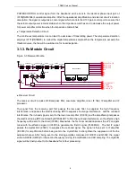
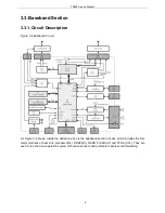
3.2. GPS Ciruit
Figure 3-5 GPS Schematic Diagram
As Figure 3-5 shows, the repeater baseband board includes the GPS module (U9) and the GPS antenna
interface J8(SMA). The corresponding equipment box is also assembled with a GPS antenna interface
which supports the outdoor active antenna. The GPS module integrates a baseband processor, LNA and
SAW. The antenna receives the 1575.42MHz GPS signal, after the inner amplification and filter process, it
will be sent to the baseband section for further calculating, to get the geographical location and time
information of the equipment. The output data information will be sent to processor (U4). Meanwhile, the
GPS module hardware will provide the one-pulse-per-second signal (1PPS) for OMAP and FPGA
respectively.
8
Содержание TR850
Страница 1: ......
Страница 45: ...TR850 Service Manual 5 4 Connection 1 2 3 4 6 8 7 5 9 10 13 14 15 16 18 17 11 12 41 ...
Страница 90: ...TR850 Service Manual Figure 1 Rx Module Top Board PCB View 86 ...
Страница 91: ...TR850 Service Manual Figure 2 Rx Module Bottom Board PCB View 87 ...
Страница 93: ...TR850 Service Manual Figure 5 Power Amplifier Module Bottom Board PCB View 89 ...
Страница 94: ...TR850 Service Manual Figure 6 Baseband Mainboard Top Board PCB View 90 ...
Страница 95: ...TR850 Service Manual Figure 7 Baseband Mainboard Bottom Board PCB View 91 ...
Страница 96: ...TR850 Service Manual Figure 8 Front Panel Top Board PCB View Figure 9 Front Panel Bottom Board PCB View 92 ...
Страница 97: ...TR850 Service Manual Figure 10 Power Board Top Board PCB View 93 ...
Страница 114: ...TR850 Service Manual Figure 16 Baseband Mainbaord Schematic Diagram 110 ...
Страница 169: ...TR850 Service Manual Figure 1 Rx module Top Board Position Mark Diagram 165 ...
Страница 170: ...TR850 Service Manual Figure 2 Rx Module Buttom Board Position Mark Diagram 166 ...
Страница 172: ...TR850 Service Manual Figure 5 Power Amplifier Module Buttom Position Mark Diagram 168 ...
Страница 173: ...TR850 Service Manual Figure 6 Baseband Mainboard Top Board Position Mark Diagram 169 ...
Страница 174: ...TR850 Service Manual Figure 7 Baseband Mainboard Buttom Board Position Mark Diagram 170 ...
Страница 176: ...TR850 Service Manual Figure 10 Power Board Top Board Position Mark Diagram 172 ...
Страница 193: ...TR850 Service Manual Figure 16 Baseband Mainboard Schematic Diagram 189 ...