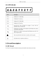


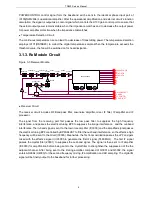


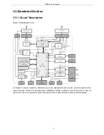


TR850 Service Manual
0R
0R
0R
1
1
1
0
Ver6.0
NULL
NULL
NULL
0
0R
0R
0R
1
1
1
1
Ver7.0
NULL
NULL
NULL
0
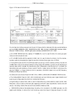
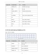
3.3.7. Baseband Board Interface and Indicator
Figure 3-16 Baseband Board Interface and Indicator
See Figure 3-16, The interfaces and indicators of banseband are as follows:
J1 is the 13.2V(+/-20%) DC input interface of the whole banseband mainboard, and the polarity
should be noted. The input circuit includes isolating magnetic inductor (L12) and chip insurance resistor
(F1).
J2 is the JTAG adjustment interface of main processor, and it is used for program simulation
adjustment.
J4 is the switch for boot mode. See
“
3.3.5
Boot Mode
”
for details.
J6
、
J7 are 12.8MHz clock and SMA offered by main board to other parts. The two signals are the same
17
Содержание TR850
Страница 1: ......
Страница 45: ...TR850 Service Manual 5 4 Connection 1 2 3 4 6 8 7 5 9 10 13 14 15 16 18 17 11 12 41 ...
Страница 90: ...TR850 Service Manual Figure 1 Rx Module Top Board PCB View 86 ...
Страница 91: ...TR850 Service Manual Figure 2 Rx Module Bottom Board PCB View 87 ...
Страница 93: ...TR850 Service Manual Figure 5 Power Amplifier Module Bottom Board PCB View 89 ...
Страница 94: ...TR850 Service Manual Figure 6 Baseband Mainboard Top Board PCB View 90 ...
Страница 95: ...TR850 Service Manual Figure 7 Baseband Mainboard Bottom Board PCB View 91 ...
Страница 96: ...TR850 Service Manual Figure 8 Front Panel Top Board PCB View Figure 9 Front Panel Bottom Board PCB View 92 ...
Страница 97: ...TR850 Service Manual Figure 10 Power Board Top Board PCB View 93 ...
Страница 114: ...TR850 Service Manual Figure 16 Baseband Mainbaord Schematic Diagram 110 ...
Страница 169: ...TR850 Service Manual Figure 1 Rx module Top Board Position Mark Diagram 165 ...
Страница 170: ...TR850 Service Manual Figure 2 Rx Module Buttom Board Position Mark Diagram 166 ...
Страница 172: ...TR850 Service Manual Figure 5 Power Amplifier Module Buttom Position Mark Diagram 168 ...
Страница 173: ...TR850 Service Manual Figure 6 Baseband Mainboard Top Board Position Mark Diagram 169 ...
Страница 174: ...TR850 Service Manual Figure 7 Baseband Mainboard Buttom Board Position Mark Diagram 170 ...
Страница 176: ...TR850 Service Manual Figure 10 Power Board Top Board Position Mark Diagram 172 ...
Страница 193: ...TR850 Service Manual Figure 16 Baseband Mainboard Schematic Diagram 189 ...