


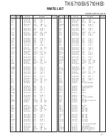

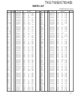
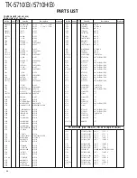
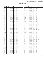

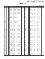
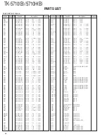

33
TK-5710
(
B
)
/5710H
(
B
)
SEMICONDUCTOR DATA
CPU:30625MGP213GP (Control unit IC703)
Pin
Port Name
I/O
Function
No.
48
DS
O
Dual band switch
49
SELF
I
Self programming mode
(L:Enable, H:Disable)
50
RDY
I
Bus control (Ready)
51
ALE
−
No connection
52
HOLD
I
Bus control (Hold)
53
HLDA
−
No connection
54
STRB
O
Shift register strobe of FPGA
55,56 NC
−
No connection
57
SCSW
O
When the scramble board is installed,
the route of AF is change.
(L:Scrambler on, H:off)
58
BCLK
O
Bus control (Base clock output)
59
RD
O
Bus control (Read)
60
BHE
−
No connection
61
WR
O
Bus control (Write)
62
NC
−
No connection
63
AUXO 1
O
Auxiliary output 1 (FPU selectable)
64
AUXO 2
O
Auxiliary output 2 (FPU selectable)
65
CHECK
I
for port check
66
CS2
O
Flash memory CS
67
CS1
O
DSP CS
68
CS0
O
Flash memory CS
69~79 A19~A9
O
Address bus 19~9
80
AM
O
AF mute (L:Unmute, H:Mute)
81
TCNT
I
Tone control input (for ANI board)
82
KEY
I
TX key input (for ANI board)
83
INH
I
Audio inhibit input (for ANI board)
84
BEEPS
O
Beep mute switch (L:Unmute, H:Mute)
85
VCC2
−
Power supply input (3.3V)
86
A8
O
Address bus 8
87
VSS
−
GND
88~95 A7~A0
O
Address bus 7~0
96
A20
O
Address bus 20
97
HINT
I(INT4) DSP HINT interrupt (L:Interrupt)
98
NC
−
No connection
99
1/2
I
Deak 1/2 L:Deak 1 (default),
H:Deak 2 (Modification:Pd
t
Pu)
100
IGN
I
Ignition sense
(L:Ignition on, H:Igniton off)
101
DRST
O
DSP reset output (L:Reset)
102
FRST
O
Flash memory reset output (L:Reset)
103
DSPINT
O
DSP interrupt output (L:Interrupt)
104~111 D7~D0
I/O
Data bus 7~0
112
STRB2
O
Shift register 2 CS
113
TAMS
O
TX audio monitor switch
(L:Disconnect, H:Connect)
114
AUX I/O 8
I/O
Auxiliary I/O 8 (FPU selectable)
115
NC
I/O
NC (for LOK customize)
116
RTCDT
I/O
RTC data I/O
117
AUX I/O 9
I/O
Auxiliary I/O 9 (FPU selectable)
118
STRB3
O
Shift register 3 CS
119
PTOS
O
for K-USA customize
1
VREF
−
A/D converter reference voltage
input terminal
2
AVCC
−
A/D converter power supply
input terminal
3
PLAY
I
Play input (for VGS) (H: Playing)
4
EI
O
Enable output for shift register of KRK
5
KCS
O
Chip select output for D/A converter
of KRK
6
NC
−
No connection
7
VOICE
O(D/A) Voice output of built-in voice guide
8
SOE
O
Shift register output enable
9
UL
I
PLL unlock (L:Unlock, H:Lock)
10
DAT
O
Common data
11
CLK
O
Common clock
12
SDA
I/O
EEPROM data
13
BYTE
I
Use as 8bit data bus (Vcc)
14
CNVSS
I
Use as memory expansion mode (Vss)
15
PCS
O
Potentiometer CS
16
XOUT
−
No connection
17
RESET
I
Reset input
18
XOUT
−
No connection
19
VSS
−
GND
20
XIN
−
Clock input, 9.216MHz (18.432MHz/2)
21
VCC1
−
Power supply input (5V)
22
NC (NMI)
I
NC
23
RXD INT
I(INT2) RXD interrupt input (L:Interrupt)
24
PSW (INT1) I(INT1) Power switch detection
(L:Power off, H:Power on)
25
INTRA
I(INT0) RTC interrupt input (L:Interrupt)
26
LD
O
DAC LD
27
BEEP
O
BEEP output
28
EP
O
PLL CS
29
AUX I/O 1
I/O
Auxiliary I/O 1 (FPU selectable)
30
AUX I/O 2
I/O
Auxiliary I/O 2 (FPU selectable)
31
STRB1
O
Shift register 1 CS
32
AUX I/O 3
I/O
Auxiliary I/O 3 (FPU selectable)
33
AUX I/O 4
I/O
Auxiliary I/O 4 (FPU selectable)
34
RXD2
I
to Display
35
TXD2
O
to Display
36
TXD1
O
to D-SUB 25pin (VGS)
37
VCC1
−
Power supply input (5V)
38
RXD1
I
to D-SUB 25pin (VGS)
39
VSS
−
GND
40
VBUSY
I
Busy input (for VGS) (H:Busy)
41
AUX I/O 5
I/O
Auxiliary I/O 5 (FPU selectable)
42
TXD0
O
to D-SUB 25pin (232C level)
43
RXD0
I
to D-SUB 25pin (232C level)
44
AUX I/O 6
I/O
Auxiliary I/O 6 (FPU selectable)
45
AUX I/O 7
I/O
Auxiliary I/O 7 (FPU selectable)
46
MM
O
MIC mute output (L:Unmute, H:Mute)
47
SBC
O
Power control output
(L:Power on, H:Power off)
Pin
Port Name
I/O
Function
No.