


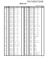

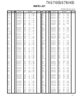
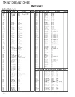
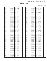


31
TK-5710
(
B
)
/5710H
(
B
)
written by the FPU (KPG-95D), and firmware program (User
mode, Test mode, Tuning mode, etc.). This data must be
rewritten when replacing the flash memory.
■
EEPROM
Note :
The EEPROM (IC701) stores tuning data (Deviation,
Squelch, etc.).
Realign the transceiver after replacing the EEPROM.
■
Real-time clock
The clock function is based on real-time clock IC (IC700).
When the power supply is off, it is backed up by an internal
secondary lithium battery.
6-2. Temperature Detection Circuit
T h e t e m p e r a t u r e d e t e c t i o n c i r c u i t d e t e c t s t h e
temperature using a temperature IC (IC702) and corrects the
thermal characteristic change of the squelch.
6-3. DSP
The DSP circuit consists of a DSP IC (IC715), a CODEC IC
(IC724) and processes the base band signal. The DSP IC op-
erates on an external clock of 9.216MHz (the same as the
CPU), the I/O section operates at 3.3V and the core section
operates at 1.5V. The DSP IC carries out the following pro-
cesses:
• C4FM encoding
• Analog FM pre-emphasis/de-emphasis
• Vocoder (IMBE) processing between audio codec and
modulation/ demodulation
• CAI processing, such as error correction encoding
• QT/DQT encoding/ decoding
• DTMF encoding/ decoding
• MSK encoding/ decoding
• 2-tone decoding
• Compressor/ expander processing
• Transmit/ receive audio filtering processing
• Microphone amplifier AGC processing
• Audio mute processing
• Modulation level processing
6-4. FPGA
The FPGA IC (IC730) I/O section operates at 3.3V and the
core section operates at 2.5V. The FPGA IC has the following
function.
• Demodulation (C4FM,CQPSK)
• Shift register (8CH)
• Level convert Buffer amplifier(5V
➝
3.3V)(9CH)
• Generates 1.536MHz for the demodulation and CODEC
7. Power Supply Circuit
The voltage is always applied from +B. D719 protects
IC705 (DFF) against overvoltage.
Pulses from power switch are fed to the IC705 clock line
and the CPU (IC703). These clock pulses reverse the output
from High (The transceiver is turned OFF) to Low (The trans-
ceiver is turned ON), but it does not reverse the output from
Low to High. The CPU (IC703) output the pulse to the S2
(SET2) terminal (pin 8) of IC705 to reverse the output from
Low to High.
IGN is connected to the R2 (RESET2) terminal (pin 10) of
IC705 and the CPU (IC703). When the IC705 reset voltage is
increased, the output changes to Low (The transceiver is
turned ON). When IGN voltage is decreased, the CPU (IC703)
output the pulse to the S2 terminal (pin 8) of IC705 to reverse
the output from Low to High after the programmed time ex-
pires (Timed power-off function).
If 24V is supplied to the transceiver by mistake, Q707
turns on, Q710 turns off, the power is forced to be turned off.
This circuit consists of IC706 (8V), IC707 (5V), IC708
(3.3V), IC710 (3.3V), IC711 (2.5V) and IC709 (1.5V).
Fig. 13
Clock diagram
CIRCUIT DESCRIPTION
CPU
EEPROM
FLASH
IC703
IC712
IC701
Fig. 12
Memory circuit
IC703
CPU
IC715
DSP
IC730
FPGA
IC724
CODEC
IC725
(2/3,3/3)
9.216MHz
9.216MHz
18.432MHz
18.432MHz
18.432MHz
IC721
X701
VCXO
IC725
(1/3)
D723
AVR
D722
SW
Q728
SW
IGN
PSW
IC703
CPU
Q705,
Q706
SW
Q711,
Q712
SW
IC705
DFF
Q704
SW
Q708
SW
D720
SW
D719
AVR
Q707
SW
D725
SW
Q710
SW
Q713
SW
SB
+B
R702
Q709
SW
D724
SW
Fig. 14
Power supply circuit