3 INDIVIDUAL SPECIFICATIONS
3-30
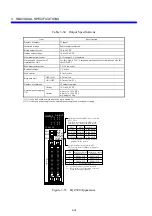
Q
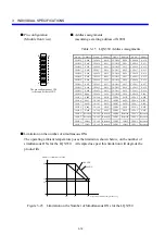
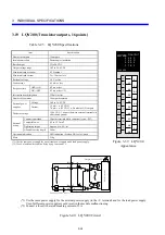
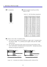
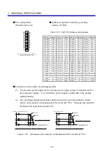
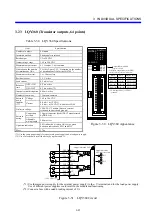
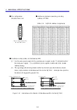
Pin configuration
Q
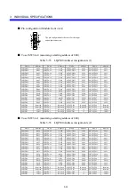
Address assignments (assuming a starting
(Module front view)
address of Y000)
Table 3-29 LQY350 Address Assignments
Pin No.
Address
Pin No.
Address
Pin No.
Address
Pin No.
Address
CN1B20
Y000
CN1A20
Y010
CN2B20 Y020 CN2A20
Y030
CN1B19
Y001
CN1A19
Y011
CN2B19 Y021 CN2A19
Y031
CN1B18
Y002
CN1A18
Y012
CN2B18 Y022 CN2A18
Y032
CN1B17
Y003
CN1A17
Y013
CN2B17 Y023 CN2A17
Y033
CN1B16
Y004
CN1A16
Y014
CN2B16 Y024 CN2A16
Y034
CN1B15
Y005
CN1A15
Y015
CN2B15 Y025 CN2A15
Y035
CN1B14
Y006
CN1A14
Y016
CN2B14 Y026 CN2A14
Y036
CN1B13
Y007
CN1A13
Y017
CN2B13 Y027 CN2A13
Y037
CN1B12
Y008
CN1A12
Y018
CN2B12 Y028 CN2A12
Y038
CN1B11
Y009
CN1A11
Y019
CN2B11 Y029 CN2A11
Y039
CN1B10
Y00A
CN1A10
Y01A
CN2B10 Y02A CN2A10
Y03A
CN1B9
Y00B
CN1A9
Y01B
CN2B9
Y02B CN2A9
Y03B
CN1B8
Y00C
CN1A8
Y01C
CN2B8
Y02C CN2A8
Y03C
CN1B7
Y00D
CN1A7
Y01D
CN2B7
Y02D CN2A7
Y03D
CN1B6
Y00E
CN1A6
Y01E
CN2B6
Y02E CN2A6
Y03E
CN1B5
Y00F
CN1A5
Y01F
CN2B5
Y02F CN2A5
Y03F
CN1B4
Reserved
CN1A4
Reserved
CN2B4
Reserved
CN2A4
Reserved
CN1B3
Reserved
CN1A3
Reserved
CN2B3
Reserved
CN2A3
Reserved
CN1B2
+V1
CN1A2
COM1
CN2B2
+V2 CN2A2
COM2
CN1B1
+V1
CN1A1
COM1
CN2B1
+V2 CN2A1
COM2
Q
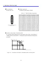
Limitation on the number of simultaneous ONs
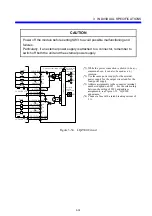
(1) Use the same power supply for the external power supply (to the +V terminal) and for
the load power supply. Use of different power supplies could result in the module
malfunctioning.
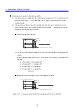
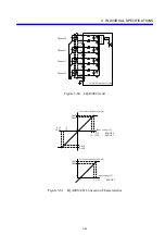
(2) The operating ambient temperature and the load current pose the limitation, shown
below, on the number of simultaneous ONs for the LQY350. Attempted use past this
limitation will degrade the product life.
55
39
0
64
32
0
42
28
24 VDC
26.4 VDC
Number of simultaneous ONs
Load current [mA]
55
39
0
50
25
0
42
20
24 VDC
26.4 VDC
Operating ambient
temperature [
]
Operating ambient
temperature [
]
Load condition: 1.6 A/common
ON condition: All outputs ON
Operating ambient temperature - Number of simultaneous ONs
Operating ambient temperature - Load current common
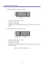
Figure 3-49 Limitation on the Number of Simultaneous ONs for the LQY350
B20
A20
A1
B1
The pin configuration of CN1 is
the same as that of CN2.
Содержание S10mini LQS070
Страница 1: ......
Страница 2: ......
Страница 19: ...This Page Intentionally Left Blank ...
Страница 30: ...1 BEFORE USE ...
Страница 37: ...This Page Intentionally Left Blank ...
Страница 38: ...2 KINDS AND SPECIFICATIONS OF I O MODULES ...
Страница 57: ...This Page Intentionally Left Blank ...
Страница 58: ...3 INDIVIDUAL SPECIFICATIONS ...
Страница 143: ...This Page Intentionally Left Blank ...
Страница 144: ...4 HANDLING ...
Страница 179: ...This Page Intentionally Left Blank ...
Страница 180: ...5 HANDLING I O DATA ON J NET ...
Страница 186: ...6 HANDLING I O DATA ON D Station ...
Страница 191: ...This Page Intentionally Left Blank ...
Страница 192: ...7 MAINTENANCE ...

