3 INDIVIDUAL SPECIFICATIONS
3-29
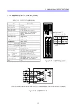
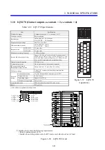
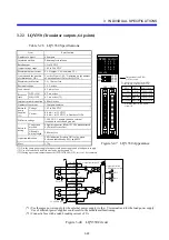
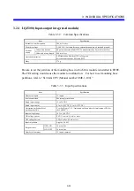
3.22 LQY350 (Transistor outputs, 64 points)
Table 3-28 LQY350 Specifications
Item Specification
Number of outputs 64
outputs
Insulation method
Photocoupler insulation
Rated output
12 to 24 VDC
Output voltage range
10.2 to 26.4 VDC
Maximum output current
0.1 A/output, 1.6 A/common (*3)
Limitation on the number
of simultaneous ONs
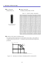
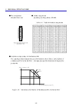
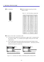
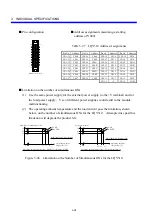
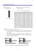
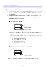
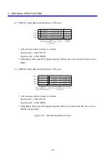
Yes (See Figure 3-49, “Limitation on the number
of simultaneous ONs for the LQY350.”)
Maximum rush current
2 A, 10 ms or less
Residual voltage
1.5 V or less
Leak current
0.1 mA or less
Response
time
OFF
→
ON
0.2 ms or less
ON
→
OFF
0.3 ms or less (*2)
Internal current dissipation 400 mA or less
Number of commons
32 outputs/common
External
power
supplies
(*1)
Voltage
10.2 to 26.4 VDC
Current
0.4 mA × n (12 VDC)
0.8 mA × n (24 VDC), n: Number of ONs
Dielectric voltage
1,500 VAC, 1 minute (between external
terminals in a batch and ground)
External
wiring
Connection
method
40-point connector (Model FCN36 manufactured
by Fujitsu Devices Inc.)
Allowable
wiring length
200 m or less
Operation indication
LED indication (lit when ON); color: green
Selection indication by SW1 and SW2
Mass 170
g
(*1) Use the same power supply for an external power supply and a load power supply.
(*2) Use of a load could result in a delay by up to around 1 s.
(*3) If using a pressure-contact connector (FCN367J040-AU/F), set it to 1.0A/common.
L
CN1B2 +V1
Load
Fuse(*2)
12-24 VDC(*1)
Output indication LED
CN1B1 +V1
CN1A2 COM1
CN1A1 COM1
L
CN1B20
000
CN1A5 01F
Output indication
LED selector switch
SW1
L
CN2B2 +V2
CN2A2 COM2
CN2A1 COM2
L
CN2B20 020
CN2A5 03F
CN2B1 +V2
SW2
Control circuit
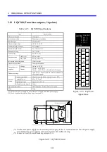
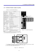
(*1) Use the same power supply for the external power supply (to the +V terminal) and for the load power supply.
Use of different power supplies could result in the module malfunctioning.
(*2) Connect a fuse with a rated breaking current of 3 A.
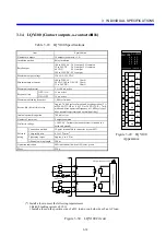
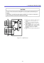
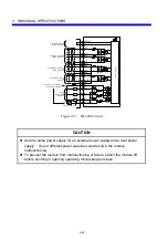
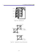
Figure 3-48 LQY350 Circuit
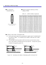
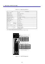
12-24 VDC
LQY350
D.OUTPUT
3
2
1
0
7
6
5
4
B
A
9
8
F
E
D
C
SW1
00-0F
10-1F
CN1
CN2
SW2
20-2F
30-3F
Output indication LED
selector switch
SW1
Left side
Display data(*)
Y000 to 00F
Y010 to 01F
(*) A starting address of Y000 is
assumed.
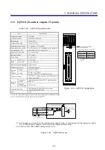
To display output data on the LED,
set the switch as instructed below.
SW2
Left side
Right side Left side
Left side
Right side
Right side Right side
Y020 to 02F
Y030 to 03F
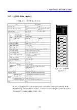
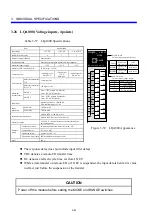
Figure 3-47 LQY350 Appearance
Содержание S10mini LQS070
Страница 1: ......
Страница 2: ......
Страница 19: ...This Page Intentionally Left Blank ...
Страница 30: ...1 BEFORE USE ...
Страница 37: ...This Page Intentionally Left Blank ...
Страница 38: ...2 KINDS AND SPECIFICATIONS OF I O MODULES ...
Страница 57: ...This Page Intentionally Left Blank ...
Страница 58: ...3 INDIVIDUAL SPECIFICATIONS ...
Страница 143: ...This Page Intentionally Left Blank ...
Страница 144: ...4 HANDLING ...
Страница 179: ...This Page Intentionally Left Blank ...
Страница 180: ...5 HANDLING I O DATA ON J NET ...
Страница 186: ...6 HANDLING I O DATA ON D Station ...
Страница 191: ...This Page Intentionally Left Blank ...
Страница 192: ...7 MAINTENANCE ...

