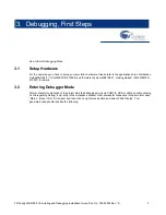
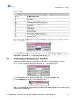
Trace
FR Family MB2198-01 Emulating and Debugging Installation Guide, Doc. No. 002-05223 Rev. *A
23
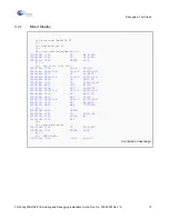
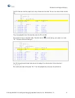
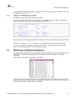
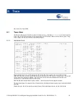
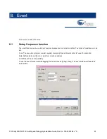
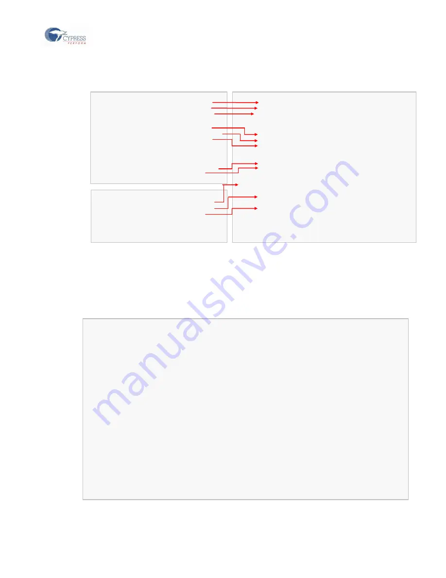
The next illustration shows the relationship between execution (trace window) and the compiled source code:
Source Code:
Trace view:
Note, you can jump to any frame by right clicking into the trace window using
Jump…
.
Also a Trace Back function is provided to see the executed instructions in history.
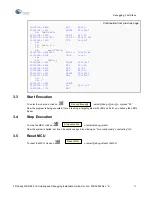
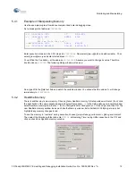
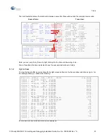
6.1.2
Cycle View
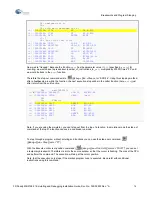
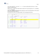
To view the trace buffer by cycle click with the right mouse button into the trace window and choose
Cycle
. For
the example above you will see the following:
In this view each executed machine cycle is displayed.
Frame no. address data (-00279 .. 00000) time stamp
-00021 : 000C0222 BTSTH #8,@R14 9,250
-00020 : read 08 at 00000482 9,050
-00019 : 000C0222 BTSTH #8,@R14 9,000
-00018 : read 08 at 00000482 8,925
-00017 : 000C0222 BTSTH #8,@R14 9,000
-00016 : read 88 at 00000482 6,800
-00015 : write 76 at 00000484 4,525
-00014 : write 01 at 00000486 1,600
-00013 : write F0 at 00000487 1,150
-00012 : write 00000000 at 0003C000 825
-00011 : 000C026E LDI:32 #0003C000,R0 1,375
-00010 : 000C02A6 LDI:32 #000C01D0,R12 625
-00009 : 000C01D0 ST RP,@-R15 50
-00008 : write 000C02AE at 0003C802 25
-00007 : write 00000487 at 0003C7FE 275
-00006 : write 00 at 00000001 325
-00005 : write FF at 00000401 800
-00004 : 000C019E ST R4,@-R15 25
-00003 : write 00004E20 at 0003C7FA 125
-00002 : write 000C01E8 at 0003C7F6 75
-00001 : write 0003C7FE at 0003C7F2 350
00000 : ----
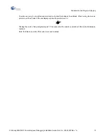
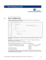
16: void wait(unsigned int a)
000C019E: 1704 ST R4,@-R15
000C01A0: 1781 ST RP,@-R15
000C01A2: 0F01 ENTER #004
17: {
18:
for (i=0; i<a; i++);
000C01A4: C000 LDI:8 #00,R0
23:
PDR1=0x00;
000C01D4: C000 LDI:8 #00,R0
000C01D6: 8B0D MOV R0,R13
000C01D8: 1A01 DMOVB R13,@001
24:
DDR1=0xFF;
000C01DA: CFF0 LDI:8 #FF,R0
000C01DC: 9B0C0401 LDI:20 #00401,R12
000C01E0: 16C0 STB R0,@R12
25:
26:
while (1)
27:
{
28:
wait(20000);
000C01E2: 9B044E20 LDI:20 #04E20,R4
000C01E6: D7DB CALL \wait
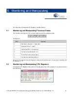
MAIN.C$23 PDR1=0x00;
: 000C01D4 LDI:8 #00,R0
: 000C01D6 MOV R0,R13
: 000C01D8 DMOVB R13,@001
-00006 : write 00 at 00000001 275
MAIN.C$24 DDR1=0xFF;
: 000C01DA LDI:8 #FF,R0
: 000C01DC LDI:20 #00401,R12
: 000C01E0 STB R0,@R12
-00005 : write FF at 00000401 675
MAIN.C$28 wait(20000);
: 000C01E2 LDI:20 #04E20,R4
: 000C01E6 CALL \wait
MAIN.C$16 void wait(unsigned int a)
\wait:
-00004 : 000C019E ST R4,@-R15 50
-00003 : write 00004E20 at 0003C7FA 125
: 000C01A0 ST RP,@-R15
-00002 : write 000C01E8 at 0003C7F6 75
: 000C01A2 ENTER #004
-00001 : write 0003C7FE at 0003C7F2 275
Содержание MB2147-01
Страница 9: ...FUJITSU SEMICONDUCTOR CONTROLLER MANUAL DSU FR EMULATOR MB2198 01 HARDWARE MANUAL CM71 00413 2E ...
Страница 10: ......
Страница 11: ...FUJITSU LIMITED DSU FR EMULATOR MB2198 01 HARDWARE MANUAL ...
Страница 12: ......
Страница 20: ...viii ...
Страница 22: ...x ...
Страница 56: ...34 CHAPTER 2 CONNECTION METHOD ...
Страница 64: ...42 CHAPTER 3 OPERATION METHOD ...
Страница 66: ......
Страница 69: ...47 APPENDIX A DSU FR Cable Specifications Figure A 2 Connector Terminal Arrangement for DSU 3 Pin 1 Pin 30 ...
Страница 76: ...54 APPENDIX B User System Specifications ...
Страница 78: ......
Страница 92: ......