


Fuji Electric Co., Ltd.
MT6M12343 Rev.1.0
Dec.-2016
1-2
Chapter 1 Product Outline
The objective of this document is introducing Fuji IGBT Intelligent-Power-Module
“Small-IPM”.
At first, the product outline of this module is described.
Secondary, the terminal symbol and terminology used in this note and the specification sheet are
explained. Next, the design guideline on signal input terminals and power terminals are shown using its
structure and behavior. Furthermore, recommended wiring and layout, and the mount guideline are given.
Feature and functions
1.1
Product concept
• 7
th
gen. IGBT technology offers high-efficiency and energy-saving operation.
• Guarantee
T
j(ope)
=150
℃
• Higher accuracy of short circuit detection contribute to expanding over load operating area.
• Compatible pin assignment, foot print size and mounting dimensions as the 1
st
gen. Small IPM series.
• Product range: 15A – 35A / 600V.
• The total dissipation loss has been improved by improvement of the trade-off between the Collector-
Emitter saturation voltage
V
CE(sat)
and switching loss.
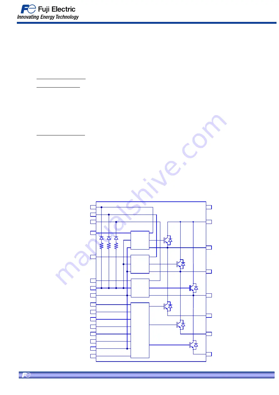
1.2 Built-in drive circuit
• Drives the IGBT under optimal conditions.
• The control IC of upper side arms have a built-in high voltage level shift circuit (HVIC).
• This IPM is possible for driven directly by a microprocessor. Of course, the upper side arm can also
be driven directly. The voltage level of input signal is 3.3V or 5V.
• Since the wiring length between the internal drive circuit and IGBT is short and the impedance of the
drive circuit is low, no reverse bias DC source is required.
• This IPM device requires four control power sources. One is a power supply for the lower side IGBTs
and control ICs. The other three power supplies are power supplies for the upper side IGBTs with
proper circuit isolation.
The IPM doesn’t need insulated power supplies for the upper side drive because the IPM has built-in
bootstrap diodes (BSD).
Fig. 1-1 Block Diagram of Internal Circuit
VB(U)
11
10
9
5
3
21
20
19
18
17
16
15
14
13
12
22
23
24
26
28
30
36
32
U
P
V
W
N(V)
N(U)
N(W)
Vcc
IN
GND
OUT
Vs
Vcc
U
IN
V
IN
W
IN
U
OUT
V
OUT
W
OUT
Fo
IS
GND
VFO
IS
COM
COM
IN(LU)
IN(LV)
IN(LW)
V
CCL
V
CCH
IN(HU)
IN(HV)
IN(HW)
VB(V)
VB(W)
TEMP
NC
V
B
7
TEMP
Vcc
IN
GND
OUT
Vs
V
B
Vcc
IN
GND
OUT
Vs
V
B
3×HVIC
LVIC
3×BSD
6×IGBT 6×FWD
1. Introduction


