


MPC563XM Reference Manual, Rev. 1
Freescale Semiconductor
835
Preliminary—Subject to Change Without Notice
Setting OPAC1 to a desired pin action and OPAC2 to no-action, and using different time bases for match1
and match2 defines a conditional OPAC1 pin action which can be blocked by match2 recognition. For
example, setting match1 on time and match2 on angle can limit the pin action to a maximum angle value.
When pulses are generated, the service is requested at the trailing edge of the pulse, after MRL2 is asserted.
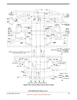
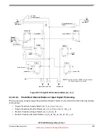
Both Match Request Modes (bm_st, bm_dt)
On an output signal, each match recognition can affect the pin state, and capture its programmed time base.
This way the pin action can be programmed separately for both match recognitions. For example, both
match recognitions can negate the signal, and service request is generated after both conditions are met.
This mechanism can set two conditions to do a required pin action, and the first recognition changes the
signal, but service is called only after both conditions occur.
When using the same time base, these modes can generate narrow pulses in any required order. For
example, in a PWM function, when duty cycle is below 50% the function can get service on the low time
and program the pulse to the required duty cycle of the high time. When duty cycle is equal or above 50%,
the function can get service on the high time and program a negative pulse with the width of the required
low time. To switch between the two states the function can program once the same transition time to
match1 and match2 with a required pin action, and on the next service program double match for the new
state.
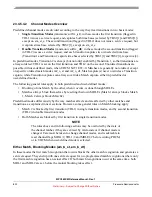
Another usage is generating a required pin action on one programmed time and service request later on
another time, after the second match recognition occurs, or capturing some timebase on one time and
generating a required signal transition and service request later.
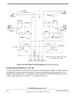
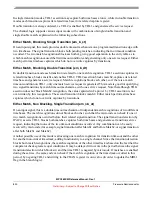
Ordered Modes with Match2 Request (m2_o_st, m2_o_dt)
The order of the match recognitions imply that OPAC1 register programmed pin action always precede the
OPAC2 register pin action. Setting OPAC1 to no-action, based on the greater-equal comparator, enables
using Match1 on one time base to delay the signal effect of Match2 on the other time base. This method
implements a conditional pulse extension or conditional delay on signal transition.
These modes can also be used for deferred pulse generation with microcode service request after its trailing
edge (if match1 condition comes after match2 condition). Another option is having match1 recognition
associated with output pin actions and match2 recognition for a timed microcode task which has to be
scheduled at a programmed time which may be delayed by the Match1 pin action.
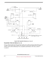
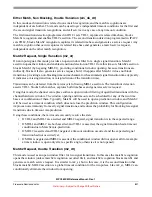
Single Match Modes (sm_st, sm_dt, sm_st_e)
There is no difference between plain and enhanced Single Match modes on an output signal.
In this mode the channel logic is functionally back-compatible to a TPU3 single match output channel.
Match1 recognition generates service request and sets the pin state according to OPAC1 register. It
captures at once the timebase selected by TBS1 in Capture1 and the timebase selected by TBS2 in
Capture2.
Содержание MPC5632M
Страница 22: ...MPC563XM Reference Manual Rev 1 22 Freescale Semiconductor Preliminary Subject to Change Without Notice ...
Страница 62: ...MPC563XM Reference Manual Rev 1 62 Freescale Semiconductor Preliminary Subject to Change Without Notice ...
Страница 92: ...MPC563XM Reference Manual Rev 1 92 Freescale Semiconductor Preliminary Subject to Change Without Notice ...
Страница 168: ...MPC563XM Reference Manual Rev 1 168 Freescale Semiconductor Preliminary Subject to Change Without Notice ...
Страница 242: ...MPC563XM Reference Manual Rev 1 242 Freescale Semiconductor Preliminary Subject to Change Without Notice ...
Страница 302: ...MPC563XM Reference Manual Rev 1 302 Freescale Semiconductor Preliminary Subject to Change Without Notice ...
Страница 410: ...MPC563XM Reference Manual Rev 1 410 Freescale Semiconductor Preliminary Subject to Change Without Notice ...
Страница 440: ...MPC563XM Reference Manual Rev 1 440 Freescale Semiconductor Preliminary Subject to Change Without Notice ...
Страница 464: ...MPC563XM Reference Manual Rev 1 464 Freescale Semiconductor Preliminary Subject to Change Without Notice ...
Страница 554: ...MPC563XM Reference Manual Rev 1 554 Freescale Semiconductor Preliminary Subject to Change Without Notice ...
Страница 590: ...MPC563XM Reference Manual Rev 1 590 Freescale Semiconductor Preliminary Subject to Change Without Notice ...
Страница 622: ...MPC563XM Reference Manual Rev 1 622 Freescale Semiconductor Preliminary Subject to Change Without Notice ...
Страница 716: ...MPC563XM Reference Manual Rev 1 716 Freescale Semiconductor Preliminary Subject to Change Without Notice ...
Страница 1114: ...MPC563XM Reference Manual Rev 1 1114 Freescale Semiconductor Preliminary Subject to Change Without Notice ...
Страница 1144: ...MPC563XM Reference Manual Rev 1 1144 Freescale Semiconductor Preliminary Subject to Change Without Notice ...
Страница 1266: ...MPC563XM Reference Manual Rev 1 1266 Freescale Semiconductor Preliminary Subject to Change Without Notice ...
Страница 1316: ...MPC563XM Reference Manual Rev 1 1316 Freescale Semiconductor Preliminary Subject to Change Without Notice ...
Страница 1348: ...MPC563XM Reference Manual Rev 1 1348 Freescale Semiconductor Preliminary Subject to Change Without Notice ...
Страница 1362: ...MPC563XM Reference Manual Rev 1 1362 Freescale Semiconductor Preliminary Subject to Change Without Notice ...
Страница 1382: ...MPC563XM Reference Manual Rev 1 1382 Freescale Semiconductor Preliminary Subject to Change Without Notice ...


