17 12-BIT A/D CONVERTER (ADC12A)
17-8
Seiko Epson Corporation
S1C17M12/M13 TECHNICAL MANUAL
(Rev. 1.2)
Bit 7
STMD
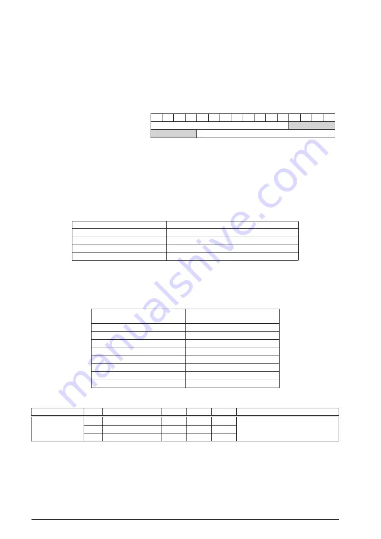
This bit selects the data alignment when the conversion results are loaded into the A/D conversion re-
sult registers (ADC12_
n
AD
m
D.AD
m
D[15:0] bits).
1 (R/W): Left justify
0 (R/W): Right justify
All the A/D conversion result registers change their data alignment immediately after this bit is al-
tered. This does not affect the conversion results.
ADC12_nADmD.ADmD[15:0] bits
15 14 13 12 11 10 9
8
7
6
5
4
3
2
1
0
Left justified (ADC12_nTRG.STMD bit = 1) (MSB)
12-bit conversion result
(LSB) 0 0 0 0
Right justified (ADC12_nTRG.STMD bit = 0) 0 0 0 0 (MSB)
12-bit conversion result
(LSB)
Figure 17.6.1 Conversion Data Alignment
Bit 6
CNVMD
This bit sets the A/D conversion mode.
1 (R/W): Continuous conversion mode
0 (R/W): One-time conversion mode
Bits 5–4
CNVTRG[1:0]
These bits select a trigger source to start A/D conversion.
Table 17.6.2 Trigger Source Selection
ADC12_nTRG.CNVTRG[1:0] bits
Trigger source
0x3
#ADTRGn pin (external trigger)
0x2
Reserved
0x1
16-bit timer Ch.k underflow
0x0
ADC12_nCTL.ADST bit (software trigger)
Bit 3
Reserved
Bits 2–0
SMPCLK[2:0]
These bits set the analog input signal sampling time.
Table 17.6.3 Sampling Time Settings
ADC12_nTRG.SMPCLK[2:0] bits
Sampling time
(Number of CLK_T16_k cycles)
0x7
11 cycles
0x6
10 cycles
0x5
9 cycles
0x4
8 cycles
0x3
7 cycles
0x2
6 cycles
0x1
5 cycles
0x0
4 cycles
ADC12A Ch.
n
Configuration Register
Register name
Bit
Bit name
Initial
Reset
R/W
Remarks
ADC12_nCFG
15–8 –
0x00
–
R
–
7–2 –
0x00
–
R
1–0 VRANGE[1:0]
0x0
H0
R/W
Note: Make sure that the ADC12_nCTL.BSYSTAT bit is set to 0 before altering the ADC12_nCFG register.
Bits 15–2 Reserved
Bits 1–0
VRANGE[1:0]
These bits set the A/D converter operating voltage range.


