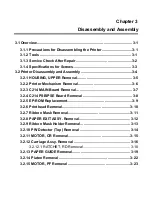
Chapter 2 Operating Principles
Rev. A
2-12
2.2.1.2 Power Supply Circuit Operation
In the power supply circuit, at first, the input AC power goes to the filter circuit, where removes the noise,
and goes to the diode bridge for full-wave rectification and is smoothed by the electrolytic capacitor. Then
it goes to the switching regulator on the primary side. This regulator uses ZC-RCC (ringing choke
converter) type and effectively gen42VDC in the secondary side. Also, +42VDC gen5VDC
by the DC-DC converter(chopper IC).
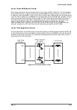
Power supply switch is mounted on the operation panel, and the PSC(power supply control signal) turns
ON/OFF the switching FET through the photo coupler in the primary side. Therefore, input voltage is in the
primary side when the AC cable is plugged in. When it is off, the current consumption is less than 1W.
Also, since C11 is constantly charged, current does not come in suddenly. PSC turns on the power
in the open state and turn off at the GND level. If the harness connecting with the operation panel is
broken or disconnected and the PSC is in the open state, the power will be always on.
+42, +5V Lines Over voltage Protection Circuit
When the output level of the +42V exceeds 55V, the switching FET in the primary side goes off via the
Zener diode (ZD52, ZD87), Transistor Q55, Q54, Q82 and photo coupler PC1.
When the output level of the +5V exceeds 10V, the switching FET in the primary side goes off via the
Zener diode (ZD53) Transistor Q55, Q54, Q82 and photo coupler PC1.
In order to recover from this, plug off the AC cable and leave the C11 about 5 minutes in order to let it
discharge electricity, and remove the cause of the over voltage and turn the power on again.
Over Current Protection Circuit
When the output current drops to 11
Ω
in case of +42V, and 4.2
Ω
in case of +5V, and lasted longer
than 1 second, over current is detected and the switching FET in the primary side goes off via
transistor Q53, Q54 Q82 and photo coupler PC1. However, if +42V or +5V shorts just before the Over
current protection circuit works, peripheral elements of Q1 are destroyed in case of +42V.
In case of +5V, peripheral elements of Q5 are destroyed. In order to recover from this, plug off the AC
cable and leave the C11 about 5 minutes in order to let it discharge electricity, and remove the cause
of the over voltage and turn the power on again.
Power Down Detector
When the output voltage of +42V becomes low and unable to maintain stable voltage, the power down
signal (PWDN) is output to the control circuit by OP. AMP (IC52B).
Output Voltage Stabilization
+42V is fed back to the primary side via Zener diode(ZD51, ZD81
∼
86 and photo coupler PC1) and
stabilizes the output voltage. +5V stabilizes the output voltage by chopper IC.
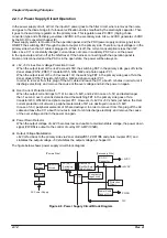
The figure below shows power supply circuit block diagram.
+5VDC
+42VDC
PC101
PWDN
PSC
[Primary Side]
[Secondary Side]
AC Power Supply
Protection
Circuit
Fuse
EMI Filter
Diode
Bridge
DC-DC
Convertor
Smoothing
Circuit
ZC-RCC
Switching
Circuit
Power Down
Sensor Circuit
Constant Vol-
tageCircuit
Half Wave
Rectifier/Smoo-
thing Circuit
Figure 2-8. Power Supply Circuit Block Diagram
Содержание LQ 670 - B/W Dot-matrix Printer
Страница 1: ...EPSON IMPACT DOT MATRIX PRINTER EPSON LQ 670 SERVICE MANUAL SEIKO EPSON CORPORATION 4007875 ...
Страница 5: ...v REVISION SHEET Revision Issued Data Contents Rev A May 28 1997 First issue ...
Страница 114: ...Chapter 6 Maintenance 6 1 Preventive Maintenance 6 1 ...
Страница 116: ...LQ 670 Service Manual Rev A 6 2 Figure 6 1 Lubrication Points ...
Страница 122: ...LQ 670 Service Manual Rev A A 5 A 2 Circuit Diagram Figure A 2 C214Main Board Circuit Diagram ...
Страница 123: ...Appendix Rev A A 6 Heat Sink Q1 D51 Figure A 3 C214PSB Board Circuit Diagram ...
Страница 124: ...LQ 670 Service Manual Rev A A 7 Heat Sink Q1 D51 Figure A 4 C214PSE Board Circuit Diagram ...
Страница 125: ...Appendix Rev A A 8 A 3 Component Layout Figure A 5 C214 Main Board Component Layout ...
Страница 126: ...LQ 670 Service Manual Rev A A 9 Figure A 6 C214 PSB Board Component Layout Figure A 7 C214 PSE Board Component Layout ...
Страница 127: ...Appendix Rev A A 10 A 4 Exploded Diagram Figure A 8 Exploded Diagram ...
Страница 128: ...LQ 670 Service Manual Rev A A 11 Figure A 9 Exploded Diagram ...
Страница 129: ...Appendix Rev A A 12 Figure A 10 Exploded Diagram ...
Страница 135: ...EPSON SEIKO EPSON CORPORATION ...

