SMARC T335x Carrier Board Hardware Design Guide, Document Revision 1.2
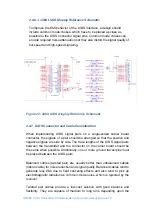
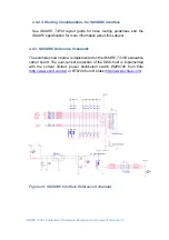
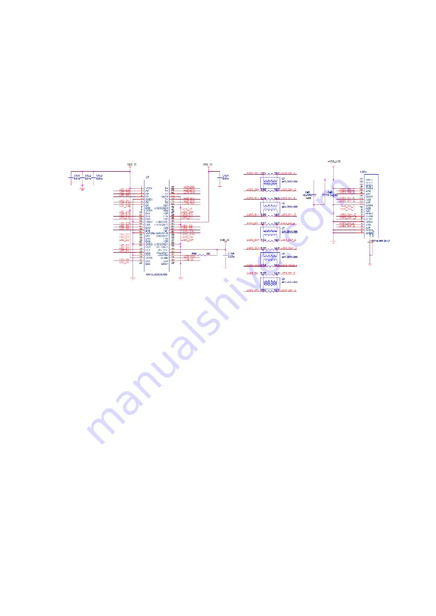
2.4.6.1. 24bit LVDS Display Reference Schematic
To improve the
EMI
behavior of the LVDS interface, a design should
include common mode chokes, which have to be placed as close as
possible to the LVDS connector signal pins. Common mode chokes can
provide required noise attenuation but they also distort the signal quality of
full-speed and high-speed signaling.
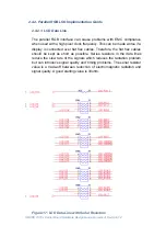
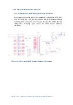
Figure 22: 24bit LVDS Display Reference Schematic
2.4.7. LVDS Connector and Cable Consideration
When implementing LVDS signal pairs on a single-ended carrier board
connector, the signals of a pair should be arranged so that the positive and
negative signals are side by side. The trace lengths of the LVDS signal pairs
between the transmitter and the connector on the carrier board should be
the same when possible. Additionally, one or more ground traces/pins must
be placed between the LVDS pairs.
Balanced cables (twisted pair) are usually better than unbalanced cables
(ribbon cable) for noise reduction and signal quality. Balanced cables tend to
generate less
EMI
due to field canceling effects and also tend to pick up
electromagnetic radiation as common-mode noise, which is rejected by the
receiver.
Twisted pair cables provide a low-cost solution with good balance and
flexibility. They are capable of medium to long runs depending upon the
Содержание SMARC T335 Series
Страница 2: ...SMARC T335x Carrier Board Hardware Design Guide Document Revision 1 2 ...
Страница 118: ...SMARC T335x Carrier Board Hardware Design Guide Document Revision 1 2 Figure 44 Power Supply Reference Schematic ...
Страница 124: ...SMARC T335x Carrier Board Hardware Design Guide Document Revision 1 2 Figure 46 SMARC T335X Module Mechanical Outline ...

