SMARC T335x Carrier Board Hardware Design Guide, Document Revision 1.2
3.1.2. Power Control Signals
The input pins listed in the following table are all active low and are meant to
be driven by OD (open drain) devices on the Carrier. The Carrier either floats
the line or drives it to GND. No Carrier pull-ups are needed. The pull-up
functions are performed on the Module. The voltage rail that these lines are
pulled to on the Module varies, depending on the design, and may be 3.3V
or
VDD_IN
.
SMARC Edge Finger
I/O
Type
Power
Rail
Description
Pin#
Pin
Name
S150
VIN_PWR_BAD#
I
CMOS
VDD_IN
Power bad indication from Carrier
board
S154
CARRIER_PWR_ON
O
CMOS
VDD_IN
Signal to inform Carrier board
circuits being powered up
P126
RESET_OUT#
O
CMOS
3.3V
General purpose reset output to
Carrier board.
P127
RESET_IN#
I
CMOS
3.3V
Reset input from Carrier board.
Carrier drives low to force a Module
reset, floats the line otherwise.
Pulled up on Module.
Driven by OD part on Carrier.
S158
VDD_IO_SEL#
IO
Strap
VDD_IN
A low logic level on this signal
indicates that the Module VDD_IO
level is configured for the default
level of 1.8V; a high value indicates
that the Module is configured for
3.3V VDD_IO.
Pullup to VDD_IN rail through a
resistance of 100K on module
P128
POWER_BTN#
I
CMOS
3.3V
Power-button input from Carrier
board. Carrier to float the line in
in-active state. Active low, level
sensitive. It is de-bounced on the
Module
Pulled up on Module.
Driven by OD part on Carrier.
Содержание SMARC T335 Series
Страница 2: ...SMARC T335x Carrier Board Hardware Design Guide Document Revision 1 2 ...
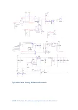
Страница 118: ...SMARC T335x Carrier Board Hardware Design Guide Document Revision 1 2 Figure 44 Power Supply Reference Schematic ...
Страница 124: ...SMARC T335x Carrier Board Hardware Design Guide Document Revision 1 2 Figure 46 SMARC T335X Module Mechanical Outline ...

