Direct Memory Access (DMA)
5-6
Copyright © 2000 ARM Limited. All rights reserved.
ARM DDI 0186A
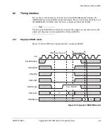
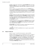
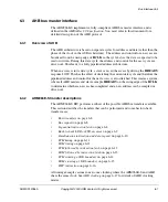
The DMA controller makes a read request by taking
DMAnREQ
LOW and asserting
DMAWait
.
DMAReady
is asserted by the ARM966E-S when the core has been stalled
on the next instruction boundary and informs the DMA controller that it can proceed
with its transfer.
Figure 5-3 on page 5-5 also shows the minimum latency between
DMAWait
being
registered HIGH and
DMAReady
being asserted is two clock cycles, when
DMAWait
is registered on an instruction boundary. The maximum latency occurs when
DMAWait
is asserted on the first cycle of an
LDM
or unbuffered
STM
AHB access. The latency in this
case can be calculated from the information in
Introduction to instruction cycle timings
The DMA controller can increment the read address on the next rising clock edge after
DMAReady
is asserted. Read data is driven on
DMARData
in the third cycle after the
read address is sampled by the ARM966E-S (one cycle to register the address, one cycle
for the RAM read and one cycle for registering the RAM read data). The first read
address,
DMAAddr
, is registered by the ARM966E-S on the next rising clock edge
after
DMAReady
is asserted.
The DMA controller has
ownership
of the RAM from
DMAReady
being asserted until
it takes
DMAWait
LOW. When
DMAWait
has been taken LOW, the DMA controller
loses ownership of the RAM.
DMAWait
must
be taken LOW at the end of a DMA
access to allow CPU flow to continue.
DMAENABLE
must be asserted one cycle prior to a request being made and can be
deasserted one cycle prior to the last read data being returned.
Note
If
DMAWait
is not asserted, the ARM966E-S does not respond to single-port RAM
DMA requests.
5.2.2
Single-port RAM writes
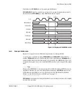
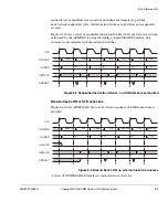
Figure 5-4 on page 5-7 shows DMA write operation to a single-port RAM.
The DMA controller requests write access to the RAM in the same way as single-port
RAM reads except that
DMAnRW
is HIGH. Because data writes are single cycle
operations, data to be written must be present in the same cycle as the address. The first
write address,
DMAAddr
, is registered by the ARM966E-S on the next rising clock
edge after
DMAReady
is asserted. The write to the RAM happens in the following
cycle, due to the single cycle latency of the input registers. The first write address,
DMAAddr
, and data,
DMAWData
, is registered by the ARM966E-S on the next rising
clock edge after
DMAReady
is asserted.
Содержание ARM966E-S
Страница 6: ...Contents vi Copyright 2000 ARM Limited All rights reserved ARM DDI 0186A ...
Страница 20: ...Introduction 1 4 Copyright 2000 ARM Limited All rights reserved ARM DDI 0186A ...
Страница 48: ...Tightly coupled SRAM 4 12 Copyright 2000 ARM Limited All rights reserved ARM DDI 0186A ...
Страница 80: ...Bus Interface Unit 6 20 Copyright 2000 ARM Limited All rights reserved ARM DDI 0186A ...
Страница 118: ...Debug Support 8 26 Copyright 2000 ARM Limited All rights reserved ARM DDI 0186A ...
Страница 130: ...Test Support 10 8 Copyright 2000 ARM Limited All rights reserved ARM DDI 0186A ...
Страница 142: ...Instruction cycle timings 11 12 Copyright 2000 ARM Limited All rights reserved ARM DDI 0186A ...
Страница 158: ...Signal Descriptions A 16 Copyright 2000 ARM Limited All rights reserved ARM DDI 0186A ...
Страница 176: ...AC Parameters B 18 Copyright 2000 ARM Limited All rights reserved ARM DDI 0186A ...

