


Preliminary Technical Data
UG-1828
Rev. PrC | Page 97 of 338
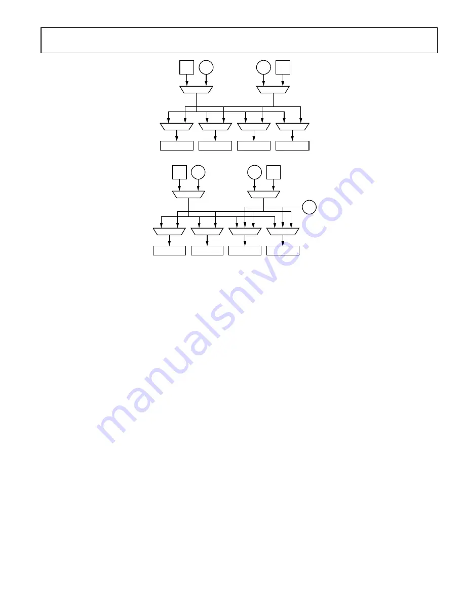
Figure 92. LO Switching Network
Figure 93. LO Switching Network (Receiver Channels Configured as Observation Receivers for Transmitter Channels)
Note that depending on the application, user has the ability to select best phase noise or best power saving options for better optimization.
The option, best phase noise, only works for LO frequency under 1 GHz.
AUXILIARY SYNTHESIZER
An auxiliary synthesizer is integrated to generate the signals necessary to calibrate the device. This synthesizer uses a single core VCO.
The reference frequency for the auxiliary synthesizer is scaled from the device clock via the reference clock generation system. The output
signal is connected to a switching network and injected into the various circuits to calibrate filter bandwidth corners, or into the receive
signal chain as an offset LO. Calibrations are executed during the initialization sequence at startup. There should be no signal present at
the receiver/observation receiver input during tone calibration time. Calibrations are fully autonomous. During the calibration, the
auxiliary synthesizer is controlled solely by the internal ARM microprocessor and does not require any user interactions. The auxiliary
LO signal is also available as an LO source for the observation receiver mixers.
EXTERNAL LO
The device is provisioned with two external LO ports. These ports are available as a pair of balls and are configured to be input for
external LO signals.
External LO can receive a signal between 60 MHz and 12 GHz through a matched differential impedance of 100 Ω and delivers a
programmable signal between 30 MHz and 6 GHz as the LO for transmitters and receivers in the device. Amplitude must be maintained
between ±6 dBm. For more information refer to External LO Port Impedance Matching Network paragraph.
Singled-ended external LO in is also supported. The matched singled-ended impedance is 50 Ω. On-chip duty cycle correction circuit can
correct limited range of external LO duty cycle error if it is not 50%.
The user can also enable external LO with 1× divider for up to 1 GHz.
Single-Ended vs. Differential External LO
Note the current eval board only supports differential external LO, however user is not restricted to use single-ended LO in their end
system. User must change clocks.ext1LoType and clocks.ext2LoType from 0 to 1. This can be found in the Enum below
enum adi_adrv9001_ExtLoType {
ADI_ADRV9001_EXT_LO_DIFFERENTIAL = 0,
ADI_ADRV9001_EXT_LO_SINGLE_ENDED = 1}
Note only frequencies from 500 MHz to 1000 MHz are supported for single-ended mode. Figure 94 shows the RF LO generation diagram.
RX2
RX2 MUX
RX1
RX1 MUX
TX2
TX2 MUX
TX1
EXT
LO1
RF
LO1
TX1 MUX
RFLO1 MUX
EXT
LO2
RF
LO2
RFLO2 MUX
24159-
076
RX2/ORX2
RX2 MUX
RX1/ORX1
RX1 MUX
TX2
TX2 MUX
TX1
EXT
LO1
RF
LO1
TX1 MUX
RFLO1 MUX
EXT
LO2
RF
LO2
RFLO2 MUX
AUX
LO
24159-
077


