UG-1828
Preliminary Technical Data
Rev. PrC | Page 50 of 338
•
Force the CSB line low and keep it low until the last byte is transferred.
•
Send the instruction word 0_000 0000 0010 1010 (the first 0 indicates a write operation) to select 0x02A as the starting address.
•
Use the next 32 clock cycles to send the data to be written to the registers, MSB to LSB for each 8-bit word.
•
Make sure the CSB line is driven high after the last bit has been sent to 0x027 to end the data transfer.
TIMING DIAGRAMS
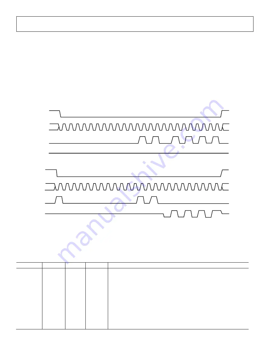
The diagrams in Figure 24 and Figure 25 illustrate the SPI bus waveforms for a single-register write operation and a single-register read
operation, respectively. In the first figure, the value 0x55 is written to register 0x00A. In the second value, register 0x00A is read, and the
value returned by the device is 0x55. If the same operations were performed with a 3-wire bus, the SDO line in Figure 24 would be
eliminated, and the SDIO and SDO lines in Figure 25 would be combined on the SDIO line. Note that both operations use MSB-first
mode and all data is latched on the rising edge of the SCLK signal.
Users should be advised, register 0x00A is not user accessible, the SPI write and read operation in Figure 24 and Figure 25 is only for the
SPI timing diagram demonstration purpose. Users can use the scratch register 0x009 for the SPI read/write test.
Figure 24. Nominal Timing Diagram, SPI Write Operation
Figure 25. Nominal Timing Diagram, SPI Read Operation
Table 13 lists the timing specifications for the SPI bus. The relationship between these parameters is shown in Figure 26. This diagram
shows a 3-wire SPI bus timing diagram with the device returning a value of 0xD4 from a test register and timing parameters marked.
Note that this is a single read operation, so the bus-ready parameter after the data is driven from the device (t
HZS
) is not shown in the
diagram.
Table 13. SPI Bus Timing Constraint Values
Parameter
Min
Typical
Max
Description
t
CP
28 ns
SCLK Period, 3-wire mode
22ns
SCLK period, 4-wire mode
t
MP
10 ns
SCLK pulse width
t
SC
3 ns
CSB setup time to first SCLK rising edge
t
HC
0 ns
Last SCLK falling edge to CSB hold
t
S
2 ns
SDIO data input setup time to SCLK
t
H
0 ns
SDIO data input hold time to SCLK
t
CO
3 ns
15 ns
SCLK falling edge to output data delay (3-wire mode)
3ns
10 ns
SCLK falling edge to output data delay (3-wire mode)
t
HZM
t
H
t
CO
(max)
Bus turnaround time after baseband processor drives the last address bit
t
HZS
0 ns
t
CO
(max)
Bus turnaround time after device drives the last data bit
WRITE TO REGISTER 0x00A – VALUE = 0x55
24159-
021
CSB
SCLK
SDIO
SDO
READ REGISTER 0x00A – VALUE = 0x55
CSB
SDIO
SCLK
SDO
24159-
022


