
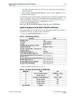

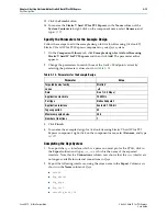


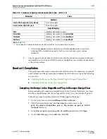


2–20
Chapter 2: Getting Started with the Stratix V Hard IP for PCI Express
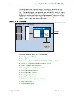
Modifying the Example Design
Stratix V Hard IP for PCI Express
June 2012
Altera Corporation
Modifying the Example Design
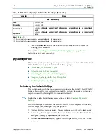
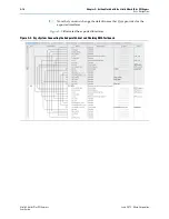
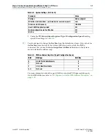
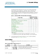
To use this example design as the basis of your own design, replace the Chaining
DMA Example shown in
with your own Application Layer design. Then,
create a Root Port BFM driver to generate the transactions needed to test your
Application Layer.
.
Figure 2–7. Testbench for PCI Express
PCB
Avalon-MM slave
Rese
t
S
tr
a
t
ix V Ha
r
d IP fo
r
PCI Exp
r
ess
S
tr
a
t
ix V FPGA
PCB
Transaction Layer
Data Link Layer
PHY MAC Layer
x8 PCIe Link
(Physical Layer)
Lane 7
(Unused)
(Unused)
Lane 6
Lane 5
TX PLL
PHY IP Co
r
e fo
r
PCI Exp
r
ess
Lane 2
Lane 3
Lane 4
Lane 1
Lane 0
TX PLL
T
r
ansceive
r
Bank
T
r
ansceive
r
Bank
S
Reconfig
to and from
Transceiver
to and from
Embedded
Controller
(Avalon-MM
slave interface)
T
r
ansceive
r
Reconfigu
r
a
t
ion
Con
tr
olle
r
Roo
t
Po
rt
BFM
npor
Rese
t
APPS
DUT
Chaining DMA
(Use
r
Applica
t
ion)