


Chapter 2: Getting Started with the Stratix V Hard IP for PCI Express
2–5
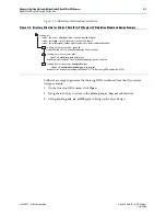
MegaWizard Plug-In Manager Design Flow
June 2012
Altera Corporation
Stratix V Hard IP for PCI Express
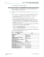
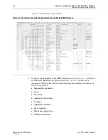
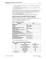
9. Specify the
Base Address Register and Expansion ROM
settings listed
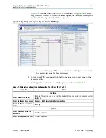
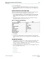
10. Under the
Base and Limit Registers
heading, disable both the
Input/Output
and
Prefetchable memory
options. (These options are for Root Ports.)
11. Specify the
Device Identification Registers
settings listed in
Table 2–3
.
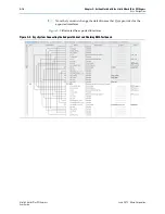
12. Specify the
Device
13. On the
Error Reporting
tab, leave all options off.
14. Specify the
Link
settings listed in
Table 2–5
.
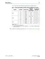
Table 2–2. Base Address Register and Expansion ROM Settings
BAR Number
TYPE
Size
0
64-bit Prefetchable Memory
256 MBytes - 28 bits
1
Disable this BAR
N/A
2
32-bit Non-Prefetchable Memory
1 KByte - 10 bits
3
Disable this BAR
N/A
4
Disable this BAR
N/A
5
Disable this BAR
N/A
Expansion ROM
Disabled
—
Table 2–3. Device Identification Registers
Register Name
Value
Vendor ID
0x00000000
Device ID
0x00000001
Revision ID
0x00000001
Class Code
0x00000000
Subsystem Vendor ID
0x00000000
Subsystem Device ID
0x00000000
Table 2–4. Device
Parameter
Value
Maximum payload size
256 bytes
Number of tags supported
32
Completion timeout range
ABCD
Implement completion timeout disable
On
Table 2–5. Link Tab
Parameter
Value
Link port number
1
Data link layer active reporting
Off
Surprise down reporting
Off
Slot clock configuration
On