Major Chips Description
2-81
2.6 YMF715B-S
YMF715-S (OPL3-SA3) is a single audio chip that integrates OPL3 and its DAC, 16 bit Sigma-delta
CODEC, MPU401 MIDI interface, joystick with timer, and a 3D enhanced controller including all the
analog components which is suitable for multi-media application. This LSI is fully compliant with
Plug and Play ISA 1.0a, and supports all the necessary features, i.e. 16 bit address decode, more
IRQs and DMAs in compliance with PC'96. This LSI also supports the expandability, i.e. Zoomed
Video, Modem and CD-ROM interface in a Plug and Play manner, and power management (power
down, power save, partial power down, and suspend/resume) that is indispensable with power-
conscious application.
2.6.1 Features
•
Built-in OPL3
•
Supports Sound Blaster Game compatibility
•
Supports Windows Sound System compatibility
•
Supports Plug
&
Play ISA 1.0a compatibility
•
Full Duplex operation
•
Built-in MPU401 Compatible MIDI I/O port
•
Built-in Joystick
•
Built-in the 3D enhanced controller including all the analog components
•
Supports multi-purpose pin function (Support 16-bit address decode, DAC interface for OPL4-
ML, Zoomed Video port, EEPROM interface, MODEM interface, IDE CD-ROM interface)
•
Hardware and software master volume control
•
Supports monaural input
•
24 mA 1TL bus drive capability
•
Supports Power Management(power down, power save, partial power down, and
suspend/resume)
..
•
+5V/ +3.3V power supply for digital, 5V power supply for analog.
•
100 pin SQFP package (YMF715-S)
Содержание 390 Series
Страница 14: ...1 2 Service Guide 1 2 System Board Layout 1 2 1 Mainboard Figure 1 1 PCB No 96183 1A Mainboard Layout Top ...
Страница 15: ...System Introduction 1 3 Figure 1 2 PCB No 96183 1A Mainboard Layout Bottom ...
Страница 96: ...2 50 Service Guide 2 3 3 Pin Configuration Figure 2 4 FDC37C67 TQFP Pin Diagram ...
Страница 97: ...Major Chips Description 2 51 Figure 2 5 FDC37C67 QFP Pin Diagram ...
Страница 102: ...2 56 Service Guide 2 3 6 Block Diagram Figure 2 6 FDC37C67 Block Diagram ...
Страница 111: ...Major Chips Description 2 65 2 4 4 3 Bottom View BGA Ball Assignments Figure 2 8 65555 BGA Ball Assignments Bottom View ...
Страница 126: ...2 80 Service Guide 2 5 4 1 Functional Block Diagram Figure 2 10 M38813 Block Diagram ...
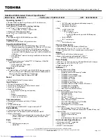
Страница 128: ...2 82 Service Guide 2 6 2 Pin Diagram Figure 2 11 YMF715 Block Diagram ...
Страница 168: ......
Страница 169: ......
Страница 170: ......
Страница 171: ......
Страница 172: ......
Страница 173: ......