


Publication No. 500-657806-000 Rev. G
Connectors and Pinouts 55
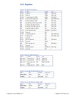
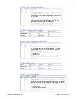
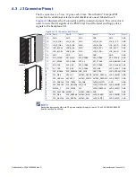
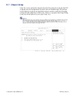
A.3 J3 Connector Pinout
The J3 connector is a 5 row, 19 pins each, 2 mm “Hard Metric” CompactPCI
connector. An additional external metal shield is also used, labeled row F.
illustrates the J3 connector and the connector pinout. This connector is
used to route the I/O signals of the PMC Site #2 and the serial and floppy drive
signals to the backplane I/O.
Figure A-3 J3 Connector and Pinout
NOTE
Backplane designs should route P3 signals straight through to rear J3. The ACC-0584/ACC-0584RC
boards can then be utilized.
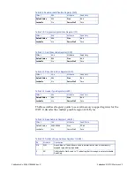
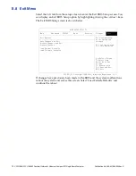
Pin No. Row A
Row B
Row C
Row D
Row E
Row F
19
GND
GND
GND
GND
GND
GND
18
LP
LPA_BI_DA-
GND
LP
LPA_BI_DC-
GND
17
LP
LPA_BI_DB-
GND
LP
LPA_BI_DD-
GND
16
LP
LPB_BI_DA-
GND
LP
LPB_BI_DC-
GND
15
LP
LPB_BI_DB-
GND
LP
LPB_BI_DD-
GND
14
GND
GND
GND
GND
GND
GND
13
SP2_RTS#B
SP1_RI#B
SP2_DSR#B
SP2_DCD#B
SP2_CTS#B
GND
12
SP1_RTS#B
SP2_DTR#B
VCC_5.0
SP1_CTS#B
LVDS_BKLTEN GND
11
SP2_TXB
SP2_RXB
SP1_DTR#B
SP1_DCD#B
LVDS_CLKAM GND
10
SP1_TXB
SP1_RXB
SP1_DSR#B
SP2_RI#B
LVDS_CLKAP GND
9
FDC_INDEX#
FDC_REDWC# USB_OC1#
USB_OC0#
LVDS_VDDEN GND
8
FDC_DIR#
KBCLK_C
AVIDEO_HSYNC AVIDEO_DDCCLK
LVDS_YAM[1] GND
7
FDC_HDSEL#
KEYDAT_C
AVIDEO_VSYNC AVIDEO_DDCDATA LVDS_YAP[1]
GND
6
FDC_RDATA#
FDC_TRK0#
SW_ON#
LVDS_BKLTCTL
GND
GND
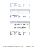
5
FDC_DRATE0
FDC_WDATA# SLP_S3#
LVDS_DDCPDATA
LVDS_YAM[2] GND
4
MSCLK_C
FDC_STEP#
N/C
LVDS_DDCPCLK
LVDS_YAP[2]
GND
3
FDC_DSKCHG# MSDAT_C
AVIDEO_GREEN GND
GND
GND
2
FDC_WP#
FDC_DRVSA# AVIDEO_BLUE
LVDS_YAM[0]
LVDS_YAM[3] GND
1
FDC_WGATE# FDC_MTR0#
AVIDEO_RED
LVDS_YAP[0]
LVDS_YAP[3]
GND
22
21
20
19
18
17
16
15
14
13
12
11
10
9
8
7
6
5
4
3
2
1