


Board to Board Connector PCB Layout
Footprint Details
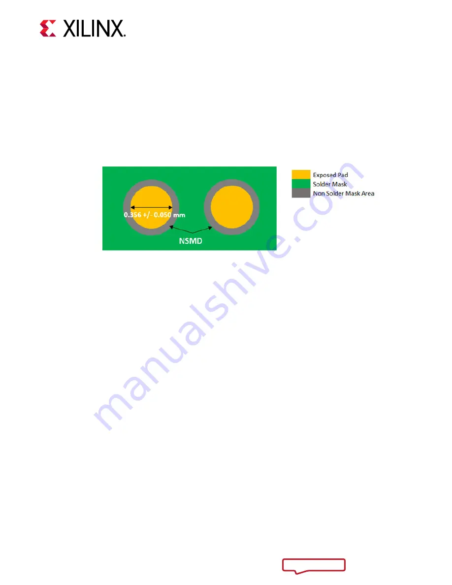
PCB pad design should be in a circular shape with diameter of 0.356 ±0.050 mm (14.0 ±2.0 mils).
Non-solder mask defined (NSMD) pad design as shown in the following figure is recommended
for better reliability performance.
Figure 7: Recommended PCB Layout for Board to Board Connector
Board to Board Connector Pad Placement
The following figure outlines the carrier card connector pads and mechanical standoff relative
placement.
Chapter 3: Mechanical Design Considerations
UG1091 (v1.0) April 20, 2021
Carrier Card Design for Kria SOM
45


