Table 4: SOM240_1 Signal Pins (cont'd)
Pin Number
Signal Name
Signal Description
D57
GTR_DP2_M2C_P
PS-GTR lane 2 TX
D58
GTR_DP2_M2C_N
PS-GTR lane 2 TX
D59
GND
Ground
D60
VCC_SOM
SOM main supply voltage, +5V
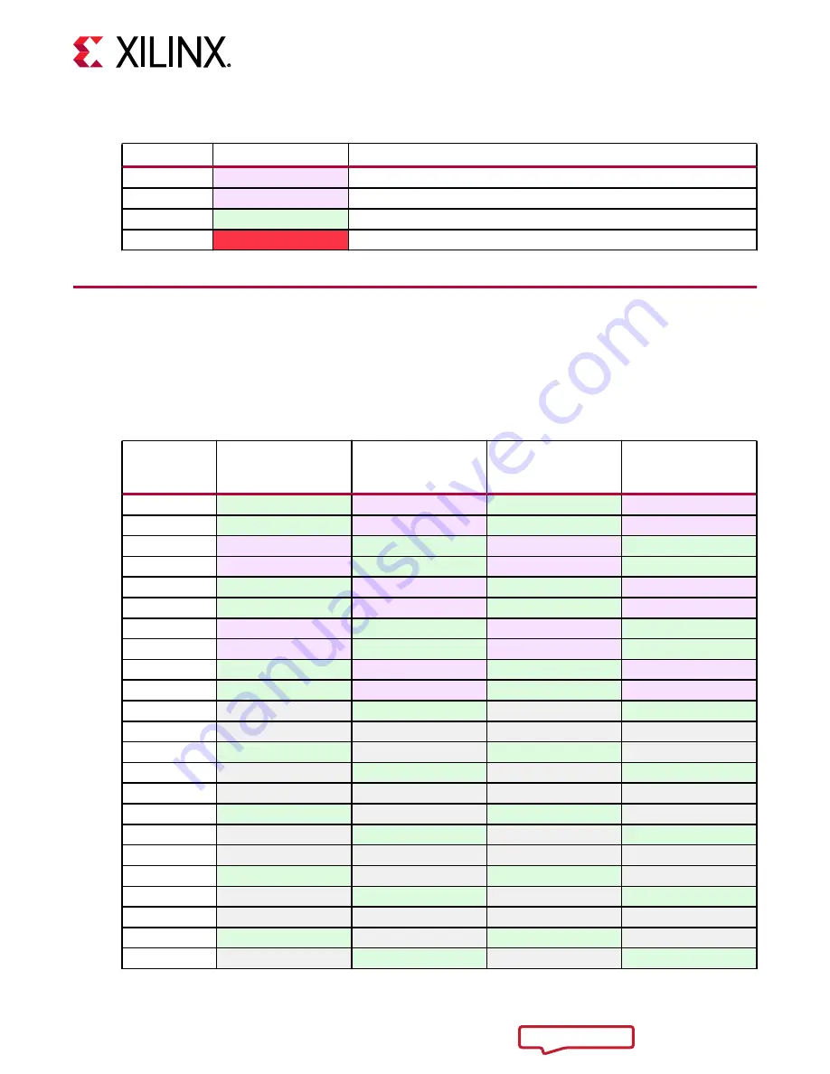
SOM240_2 Connector Pinout
The SOM240_1 connector provides access to two HPIO bank 65 (HPB), HPIO bank 64 (HPC),
HDIO bank43 (HDB, HDIO bank 44 (HDC), and the PL GTH Quad.
Table 5: SOM240_2 Connector Pinout
Connector
Row/ Pin
Number
A
B
C
D
1
GND
GTH_DP2_C2M_P
GND
GTH_DP1_C2M_P
2
GND
GTH_DP2_C2M_N
GND
GTH_DP1_C2M_N
3
GTH_DP3_C2M_P
GND
GTH_REFCLK0_C2M_P
GND
4
GTH_DP3_C2M_N
GND
GTH_REFCLK0_C2M_N
GND
5
GND
GTH_DP2_M2C_P
GND
GTH_DP3_M2C_P
6
GND
GTH_DP2_M2C_N
GND
GTH_DP3_M2C_N
7
GTH_REFCLK1_C2M_P
GND
GTH_DP1_M2C_P
GND
8
GTH_REFCLK1_C2M_N
GND
GTH_DP1_M2C_N
GND
9
GND
GTH_DP0_C2M_P
GND
GTH_DP0_M2C_P
10
GND
GTH_DP0_C2M_N
GND
GTH_DP0_M2C_N
11
HPB15_CC_P
GND
HPB09_P
GND
12
HPB15_CC_N
HPB10_CC_P
HPB09_N
HPB01_P
13
GND
HPB10_CC_N
GND
HPB01_N
14
HPB08_P
GND
HPB14_P
GND
15
HPB08_N
HPB07_P
HPB14_N
HPB00_CC_P
16
GND
HPB07_N
GND
HPB00_CC_N
17
HPB12_P
GND
HPB02_P
GND
18
HPB12_N
HPB05_CC_P
HPB02_N
HPB_CLK0_P
19
GND
HPB05_CC_N
GND
HPB_CLK0_N
20
HPB06_P
GND
HPB13_P
GND
21
HPB06_N
HPB11_P
HPB13_N
HPB04_P
22
GND
HPB11_N
GND
HPB04_N
23
HPB16_P
GND
HPB_18_P
GND
Chapter 2: Electrical Design Considerations
UG1091 (v1.0) April 20, 2021
Carrier Card Design for Kria SOM
17