VXI Technology, Inc.
56
SMP7500 Theory of Operation
VXI
I
NTERFACE
D
EVICE
T
RANSFERS
(O
UTPUT
M
ODE
)
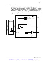
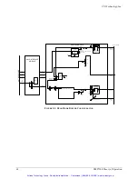
When write transfers to the UUT are desired the SMP7500 will source data out to the UUT. If
output clocks are required they must be setup and enabled to drive the F/P CLK lines. Data will be
latched into the I/O Data Buffer upon a VXI register write to the PORT’s location.
D
IRECTION
Direction of transfer is controlled either from the front panel connector or from the PORT’s
Control Register PORT Inn/Out Select Bit. Controlling the direction of the PORT
programmatically overrides the F/P CLK lines. If the direction of the PORT is programmatically
set to an output, the PORT will be an output. The PORT Inn/Out Select Bit is OR’ed with the
corresponding I/O signal from the front panel connector.
C
LOCK
E
NABLE
Output clock enabling is accomplished when the SMIP
II
module receives the VXI register write
that sets the PORT’s Control Register PORT Output Clock Enable Bit. The Output Clock Polarity
and source are set in the same fashion.
D
ATA
L
OAD
Loading of data into the I/O Word Buffer occurs when the SMIP
II
receives the VXI register write
to one of the PORT registers. The I/O buffers need to be setup for the desired mode of operation
prior to writing to the PORT Registers via the PORT Control Registers.
Artisan Technology Group - Quality Instrumentation ... Guaranteed | (888) 88-SOURCE | www.artisantg.com

