www.vtiinstruments.com
SMP7500 Programming
51
R
EGISTER
A
CCESS
E
XAMPLES
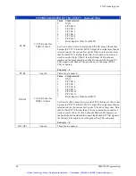
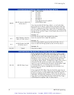
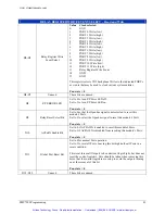
The SMP7500 module supports direct register access for very high-speed data retrieval. The
register map is as specified in Table 3-2.
As can be seen from the register map in Table 3-2, each 16-bit wide register is shared by two
ports. Therefore, in order to program a particular port, it must be ensured that the value of the
other port is untouched. This can be ensured by reading the value of the register and OR’ing the
obtained value with the value to be programmed. This final value can then be written at the
correct offset. This is true assuming that the function used to write to the register performs 16-bit
writes.
Similarly, when a register is read, it provides the data values of two ports. Therefore, the
unwanted value must be OR’ed with a proper mask. This is again assuming that the function used
to read the register performs 16-bit reads.
Example 1:
For example in order program Port 0:
a) First the register value at offset 0x00 is read. It will be assumed that the value read is as given
below:
1111000010101010
(in binary format)
The lower 8 bits are the current value for Port 1. In order to maintain its value, an appropriate OR
operation is required. A bit-shift operation may also be required depending on the port to be
written to.
For example, if the new value to be written to Port 0 is 00001111, then the final value to be
written to the register is
(1111000010101010 | (00001111 << 8))
Example 2:
For example in order read Port 0:
Read the register at offset 0x00. This presents the values of Ports 0 and 1. However, since the
value of Port 0 is of interest, the following steps must be followed:
a) Read the register at offset 0x00. It will be assumed that the value read is as shown below:
1010000011110000
(in binary format)
b) Since the upper 8 bits are of interest, an appropriate mask has to be applied and the value
right shifted.
The data value of port 1 is
((1010000011110000 | 0xFF00) >> 8)
The Model SMP7500 Digital I/O Module supports direct access to the twelve 8-bit data ports via
the A24/A32 device dependent memory space of VXIbus interface. The specific registers are
located in A24/A32 Memory. Refer to Table 3-2 showing the A24/A32 Memory Map for the
SMP7500.
Artisan Technology Group - Quality Instrumentation ... Guaranteed | (888) 88-SOURCE | www.artisantg.com


