background image


      XIIMUS 4K CL User Manual.    Model: 4096CT.                                                                            Version 1.4


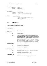
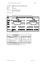
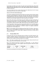
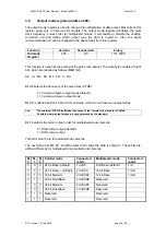
10.2.2  B2: 

Multiplexed colour channels output modes 

 
Version: 2.02 
Date: 

9 June 2006 

 
Firmware L1:  R19 for 8.3 MHz models 
 

K01 for 16.7 MHz models 


Firmware L2:  D13 
 
 
Notes: 

swap letters R and B of data values for BGR output sequence 


FVAL is constantly HIGH. DVAL is identical to LVAL. 


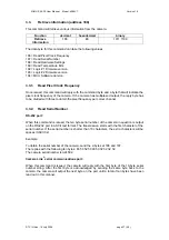
TVI XIIMUS 4096CT       

Multiplexed Output Modes 


Symbol


Parameter


Min.


Max.


Unit


T1 

NewLine low (CC1) 

80 

ns 


T2 


Line Scan Period                         
                            3 x 

4096

 pixels           8.3   MHz

                                                              16.7  MHz


502 
252 


µs 

T3 

Delay to Change of Line                       8.3    MHz 
            

1

                                              16.7  MHz 

0.7 
0.8 


0.9 
0.9 


µs 

T4 

Effective Integration Time 

µs 

T5 

Delay to Exposure Control active (CC2 … CC4) 

µs 


1

 Please note the jitter of five STROBE clock periods. 

    There is no jitter, if the Line Scan Period equals a multiple of six pixel clocks.


© TVI Vision, 14 July 2006                                                                                                      page 31 ( 56 )   

Summary of Contents for XIIMUS 4096CT

Page 1: ...information in this document without prior notice TVI Vision Oy will not take any responsibility for any damage caused by possible inaccuracies or faults in the equipment This document may not be copied without the written consent of the TVI Vision Oy An un authorised use or distribution of this document to a third party is prohibited 14 07 2006 11 42 00 ...

Page 2: ...s multiplexed output 3 x 512 pixel models 1 2 29 June 2004 jjl nr all models from 512 to 4K colour pixels 1 3 6 July 2006 jjl nr 4K specific version Description of CC1 to CC4 signals Update on specifications New timing diagrams Update on serial communications Several minor corrections Appendix C Serial communications Firmware updates D11 Æ D13 and D12 ÆD14 Read out of temperature status Time out a...

Page 3: ...ECTIVE 89 336 EEC EMC ELECTROMAGNETIC COMPATIBILITY WE HEREWITH DECLARE THAT THIS PRODUCT COMPLIES WITH THE FOLLOWING PROVISIONS APPLYING TO IT Emission CISPR 22 1997 Immunity IEC 61000 6 2 1999 APPLICABLE PATENTS FI 97264 US 6 476 870 EP 0 788 709 CA 2 203 835 JP 3626998 TVI Vision 14 July 2006 page 3 56 ...

Page 4: ...CONSIDERATIONS 21 7 1 SPECTRAL RESPONSE 21 7 2 SELECTION OF OPTICS 22 7 2 1 Modulation transfer function 22 7 2 2 Resolution and field of view 23 7 2 3 Depth of field and working aperture 23 8 LIGHTING 25 8 1 SPECTRAL RADIANCE AND COLOUR TEMPERATURE 25 8 2 UNIFORMITY OF LIGHTING 25 9 TECHNICAL SPECIFICATIONS 27 10 APPENDIXES 28 10 1 APPENDIX A CAMERA LINK OUTPUT BIT PORT ASSIGNMENTS 29 10 2 APPEND...

Page 5: ...gh sensitivity and precise colour recognition The applications for the XIIMUS cameras include web inspection inspection of natural materials like food wood ore minerals and lumber recycling quality control in printing processes texture recognition CUSTOMER SUPPORT If you need to contact the manufacturer directly please send your questions preferably by email to TVI Vision They will be forwarded to...

Page 6: ...fully accessed from the front If there are small amounts of contaminants or dust on the prism surface use a clean lint free cotton swab or other non abrasive medium dipped in acetone or pure alcohol to clean prism surface Shake excess solvent off before touching the surface of the prism to avoid streaking TVI Vision is not responsible for any scratches or damage inflicted by the customer to the fr...

Page 7: ...rate the camera in the vicinity of strong electromagnetic fields above the require ments of CE conformity This may cause erroneous operation of the camera Transporting Preferably transport the camera in its original packaging If the package is discarded please package with care in thick layer of soft preferably anti static material when transporting Do not use material that allows the camera to dr...

Page 8: ...ixels of all the three sensors are very precisely positioned optically in the same place This makes the colour analysis simpler and does not require any line matching or synchronising of separate colour lines The resolution of the camera is the same as for the individual CCD array R G B RGB color line 3 x CCD Figure 3 2 Alignment of the CCD linear arrays 3 2 Camera Operation The CCDs convert incom...

Page 9: ... the camera responds by sending out the digital data stream of the previous line scan period time The output frequency is constant The distance in time between two NewLine edges can be set to any value above the specified minimum The reciprocal of this time is the line rate Hz The XIIMUS cameras have been optimised for high speed applications Therefore best per formance is achieved at line rates o...

Page 10: ...e integration time can be precisely controlled But if the line rate is determined by encoder input the integration time can best be kept constant by using the encoder input pulse for generating the ExpCtrl signal The NewLine pulse is sent after a constant delay appendix F The XIIMUS camera is constantly monitoring all the internal supply voltages and the internal temperature of the camera Temperat...

Page 11: ...th also includes an input clamp circuit that is not drawn in the illustra tion The input clamp circuit removes the CCD s optical black offset to maximise system headroom and the effect of gain change on the black level The effect of this circuit causes the digital output data to start from zero when the CCD is exposed to dark If desired the dark level register can be used to set a positive offset ...

Page 12: ... 3 RRR GGG BBB RRR GGG BBB R Within a single colour pixel the data is ordered into a multiplier and an offset The multiplier consists of 14 bits and the offset of 10 bits Thus the three bytes that make up the correction data for one colour pixel are internally divided on a bitwise level as follows R byte 0 R byte 1 R byte 2 Multiplier Offset 13 12 11 10 9 8 7 6 5 4 3 2 1 0 9 8 7 6 5 4 3 2 1 0 Plea...

Page 13: ...cause the original data is scaled up stretched to cover a larger range By altering the content of the shifter register it is possible to reset the multiplier unity level to any power of two between 128 and 16384 Please notice that setting this register to 16384 will not permit any amplification but on the other hand will permit fine resolution attenuation Also setting this register to low values w...

Page 14: ...ect location depending on the unity mul tiplier level set in the shifter register Example The shifter register is set to 7 which equals 128 as a unity multiplier The digital gains are set to 7 as well which equals 128x digital gain In this case the result after the multiplication is shifted up 14 positions which means the lowest 12 bits of the resulting 26 bits are shifted to the data output Examp...

Page 15: ... scaled Thus at the beginning of the red line the lowest pixel value at level L2 has to be mul tiplied with a multiplier Rx so that it equals line L1 Accordingly at the start of blue channel line the line L3 has to match line L1 for the camera to be in white balance As illustrated in fig 4 4 the blue channel will have the largest multipliers and the centre of the red channel line will have multipl...

Page 16: ...ra Link connector according to the specifica tions The port is set according to the order Ask for detailed instructions if you want to swap it later on Six indicator LEDs on the right hand side show the status of the camera Figure 5 1 The rear panel layout for Camera Link models 5 1 Power input The connector is labelled as PWR IN A power cable is included in all the camera ship ments The bottom mo...

Page 17: ... the camera operation has been shut down After the external tem perature has fallen into the specified range switch the power once OFF and then ON again The camera did not start up properly Check the input power lines and the POWER LED The power supply must be able to supply enough current quickly at beginning of the power up STATUS 1 green ON Correction unit PCU is enabled OFF Correction unit PCU...

Page 18: ... delay period is the line rate CC2 Exposure Control Red or all channels exposure control signal for the Red channel the effect for this is defined by the mode that is selected via RS 232 interface or Camera Link serial port as default this signal is common to all the three CCDs a low level resets all the pixels should be constantly high if full time exposure is needed a constant 0 results in dark ...

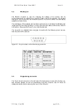
Page 19: ...oth options Please specify the port when ordering cameras The connector is a standard 9 pin plug type connector with the following pin out as seen from the behind of the camera Figure 5 2 The pin numbers of the RS 232 plug connector Table 5 1 Pin out of the RS 232 connector PIN NAME DIRECTION DESCRIPTION 1 2 RD input Receive Data 3 TD output Transmit data 4 5 SG Signal Ground 6 7 RTS output Reques...

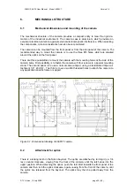
Page 20: ... the mounting holes at the side of the camera body First possibility is to fasten the camera with four screws to a special mounting stand The second option is to use a normal camera tripod using a standardised tripod at tachment 1 4 20 UNF The third is to use two M6 threaded holes to attach the camera to any application specific frame or support Figure 6 1 Dimensional drawing of 4096CT camera 6 2 ...

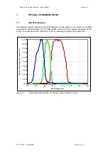
Page 21: ...urements of the beam splitter prism and the spectral sensitivity of the CCDs Channels have been matched to 100 by selecting the gains of the channels 0 00 10 00 20 00 30 00 40 00 50 00 60 00 70 00 80 00 90 00 100 00 300 400 500 600 700 800 900 1000 Wavelength nm Typical relative spectral response Figure 7 1 Typical spectral response of complete camera without a lens TVI Vision 14 July 2006 page 21...

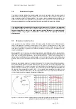
Page 22: ...of lines per mm after they have been projected In general it is defined as fidelity of the image in comparison to the object being imaged Maximum MTF is 1 0 but due to optical imperfections and diffraction this is impossible to reach MTF at large apertures f1 0 2 8 is limited by optical imperfections which vary a lot from lens to lens and manufacturer At small apertures f11 f32 lens performance is...

Page 23: ...When using large apertures large field of view and depending on the quality of the objective used image quality can be reduced at the edges due to optical limitations The focal length of optics required for imaging can be calculated from the following formula d x L F where FOV F focal length of the lens mm d distance to object mm L length of the CCD 40 96 mm FOV field of view object size mm Exampl...

Page 24: ...harp edge turns light slightly off The aperture forms such a sharp edge and light closest to the edges causes fuzziness in the image When using wider apertures the percentage of light passing along the edges decreases in relation to light passing through the centre So at small apertures the ratio of light passing close to the edges increases and thus small apertures result in a lot of diffraction ...

Page 25: ...hen lighting colour temperature is close to or over 4000K High quality colour images require a colour temperature of around 6500K or more Lighting that generates a lot of IR or UV might affect the working of the CCD sensors and should be filtered out or the source of lighting must be chosen so that the content of unde sired wavelengths is minimised 8 2 Uniformity of lighting Uniformity of lighting...

Page 26: ... qualification to be done this aspect should be carefully considered The temperature dependency of the chosen light source should be verified For example fluorescent tubes have a relatively high relation between the operating temperature and both the intensity and the proportion of colour output while all TVI XIIMUS cameras have almost no changes in their performance TVI Vision 14 July 2006 page 2...

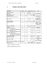
Page 27: ...thin 20 to 36 V Power consumption 12 17 26 W Weight m 1 3 kg without lens Operating temperature data rate 25 MHz per CCD Top 5 35 C 41 to 95 F Operating temperature data rate 25 MHz per CCD Top 5 20 C 41 to 68 F Operating temperature data rate 25 MHz per CCD with integrated cooling option Top 5 50 C 41 to 122 F Storage temperature Tst 10 55 C 14 to 131 F Humidity operating 5 85 relative non conden...

Page 28: ...mera Link output bit port assignments B Timing diagrams B1 Parallel colour channels output modes B2 Multiplexed colour channels output modes C Serial communications D Model numbers E Ordering codes F Application notes G Cooling Option TVI Vision 14 July 2006 page 28 56 ...

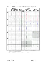
Page 29: ...0 8 10 8 5 9 9 11 9 11 9 6 10 10 10 10 B 7 11 11 11 11 0 4 4 2 0 2 0 1 5 5 3 1 3 1 2 6 6 4 2 4 2 3 7 7 5 3 5 3 4 8 8 6 4 6 4 5 9 9 7 5 7 5 6 10 10 8 6 8 6 C 7 11 11 9 7 9 7 0 2 2 0 10 8 1 3 3 1 11 9 2 2 4 2 10 3 3 5 3 11 4 2 6 4 6 4 5 3 7 5 7 5 6 X 8 6 8 6 D 7 X 9 7 9 7 0 10 8 2 0 1 11 9 3 1 2 10 4 2 3 11 5 3 4 2 6 4 6 4 5 3 7 5 7 5 6 X 8 6 8 6 E 7 X 9 7 9 7 0 2 2 0 10 8 1 3 3 1 11 9 2 2 4 2 10 3 ...

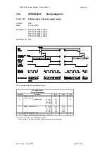
Page 30: ... XIIMUS 4096CT Parallel Output Modes Symbol Parameter Min Max Unit T1 NewLine low CC1 80 ns T2 Line Scan Period 3 x 4096 pixels 20 MHz 25 MHz 33 3 MHz 40 MHz 210 168 126 105 µs T3 Delay to Change of Line 20 MHz 25 MHz 1 33 3 MHz 40 MHz 0 39 0 45 0 52 0 54 0 44 0 49 0 55 0 565 µs T4 Effective Integration Time 2 µs T5 Delay to Exposure Control active CC2 CC4 2 µs 1 Please note the jitter of one STRO...

Page 31: ... is identical to LVAL TVI XIIMUS 4096CT Multiplexed Output Modes Symbol Parameter Min Max Unit T1 NewLine low CC1 80 ns T2 Line Scan Period 3 x 4096 pixels 8 3 MHz 16 7 MHz 502 252 µs T3 Delay to Change of Line 8 3 MHz 1 16 7 MHz 0 7 0 8 0 9 0 9 µs T4 Effective Integration Time 2 µs T5 Delay to Exposure Control active CC2 CC4 2 µs 1 Please note the jitter of five STROBE clock periods There is no j...

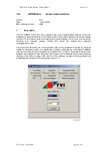
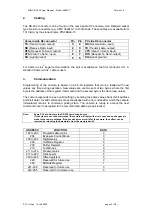
Page 32: ...s are included please contact TVI Vision for details and upgrades sales tvivision com This document describes the communication and all the available functions as low level details for developing users own application software Alternatively a Windows software with source codes and documentation is available from TVI Vision Separate versions of the software are available for use with either the Cam...

Page 33: ...of the register command and the second byte is the data new value The camera responds to each valid setting by sending the same values back 8 bit address and 8 bit data Invalid commands are acknowledged with error codes after which the camera immediately returns to command polling state The camera is ready to accept the next command once it has replied to the command and data byte pair issued Note...

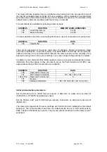
Page 34: ...e contents of the selected memory bank or the current settings in use see corresponding sections for details In addition to the commands that modify registers there are several commands that retrieve information from the camera or they are used to set up the Pixel Correction Unit PCU see appropriate sections of this document for more details ADDRESS FUNCTION DATA 180 Reserved for future use 0 181 ...

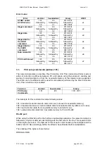
Page 35: ... serial port Loading and saving of correction data to or from the nonvolatile memory of the camera is also supported The written set of coefficients will be used for calculations performed by the Pixel Correction Unit if the correction unit is enabled Function decimal hexadecimal binary PCU Setup Commands 181 B5 1011 0101 The data byte for this command can take following values 181 download correc...

Page 36: ...ordering and the amount of bytes to be received The third operation will retrieve previously saved correction data from the nonvolatile memory to the camera for use The loaded set of coefficients will be the one used for calculations performed by the Pixel Correction Unit if correction is enabled This operation behaves the same with both communications ports Note The load operation will be automat...

Page 37: ...he pixel frequency per colour channel 3 3 2 Read Serial Number RS 232 port When this command is issued the ten byte serial number of the camera in question is output on the RS 232 port in ASCII text format The transmission starts with the first character of the serial number If the serial number is shorter than 10 characters the extra characters will be spaces ASCII 32 Example To obtain the serial...

Page 38: ...camera V1 V0 Interpretation 0 0 1024 pixels 0 1 2048 pixels 1 0 4096 pixels 1 1 512 pixels Please contact TVI if this setting is not correct as it will affect correct operation of the camera The second data byte is reserved for future use 3 3 4 Read Temperature Bits This command will reply with the command byte and a second byte that will indicate the internal temperature level as follows X X X X ...

Page 39: ...and and data byte pairs See below in Memory functions for more details 3 5 Memory functions addresses 190 and 191 The internal nonvolatile memory of the camera is divided into 64 so called memory banks Each bank can save the status of all the sixty four addresses 192 to 255 registers Each register is made of 8 bits Values can only be loaded from the memory as complete sets of 64 registers memory b...

Page 40: ...ort Communication ends when all 64 command and data byte pairs have been output and acknowledged on the serial port NOTE Data storage is guaranteed only up to 100 000 SAVE commands All the memory banks have been preset to use the initial communications port If the port has been changed after delivery loading of any of these banks will reset the port back to the initial setting unless the bank has ...

Page 41: ... controls Channel odd even decimal hexadecimal binary RED odd 194 C2 1100 0010 even 195 C3 1100 0011 GREEN odd 198 C6 1100 0110 even 199 C7 1100 0111 BLUE odd 202 CA 1100 1010 even 203 CB 1100 1011 Example 1 How to set the blue channel to maximum gain Set the selected COM port of the PC to 19200 8 N 2 Set the analog gain of odd pixels of the blue channel to maximum value in the advanced user mode ...

Page 42: ... be always inactive respective channel is never reset by the Exposure Control or to be always active pixels are reset all the time by the Exposure Control this results to a dark output value for the selected channel The third choice is a test mode where the pixels are reset until the end of the LineValid signal This is a constant time Thus the amount of exposure will depend on the line rate only s...

Page 43: ...led as follows MSB first X X X X X D2 D1 D0 The last 3 bits are used for each colour channel see table below As default these are all zeros and there is no need to change them due to the sensitivity of the camera They can though be used in cases where lighting is insufficient or to compensate for reducing working aperture size to decrease blur in the image D2 D1 D0 Function 0 0 0 1x digital gain i...

Page 44: ...output mode default 1 Camera at slower output mode Bit SP is defined as Don t Care X for cameras which do not have two output modes Note The minimum STRB PixelStrobe frequency of the Camera Link standard is 20 MHz Possible slower output modes are not guaranteed by the standard Bit CL selects the colour output order for multiplexed mode cameras 0 RGB colour output default 1 BGR colour output This b...

Page 45: ...ion Unit The setting of this register defines which digital number is interpreted as multiplying with unity This register setting is meaningful only when correction is enabled Function decimal hexadecimal binary Shifter register 209 D1 1101 0001 The data byte consists of eight bits which are labelled as follows MSB first X X X X X D2 D1 D0 D2 D1 D0 Unity level of multiplier 0 0 0 16384 0 0 1 8192 ...

Page 46: ...e 255 followed by a full ramp in the next pixels The same applies to pairs of G1 and G0 as well as for B1 and B0 Bit AC selects the auto clocking mode 0 normal operation default 1 Auto clocking mode enabled In the auto clocking mode the camera doesn t need a grabber or trigger to request a line Lines are constantly output at a fixed frequency when this mode is enabled The data output is valid data...

Page 47: ...data if desired If this parameter is set the dark level of channel in question will have an offset equal to the dark level setting Function decimal hexadecimal binary Dark Level Red odd channel 217 D9 1101 1001 Dark Level Red even channel 218 DA 1101 1010 Dark Level Green odd channel 219 DB 1101 1011 Dark Level Green even channel 220 DC 1101 1100 Dark Level Blue odd channel 221 DD 1101 1101 Dark L...

Page 48: ...s associated with the serial communications port The setting of this register defines which baud rate will be used for serial communication Both communications ports can be individually set to the desired baud rate Function decimal hexadecimal binary Bit Rate register 230 E6 1110 0110 The data byte consists of eight bits which are labelled as follows MSB first PZ X X X C1 C0 R1 R0 Bit PZ enables t...

Page 49: ...Please note that if the baud rate is changed the new setting must be saved to a memory bank using the new baud rate If the new baud rate is desired to be available at power up this new setting must be saved memory bank 0 3 16 Customer Registers addresses 240 255 The last sixteen 8 bit registers of each memory bank are reserved for customer use These registers can contain any information related to...

Page 50: ...nels blank for RGB channels 4 Pixel size of the sensors 14 for cameras with 14 µm square sensors available for 512 1K and 2K pixel resolutions blank for all 10 µm models 5 Read out rate of each colour channel 40 40 MHz for parallel output only Camera Link and LVDS 33 33 MHz for parallel output only Camera Link and LVDS 25 25 MHz for parallel output only Camera Link and LVDS 20 20 MHz for parallel ...

Page 51: ...0 µm 14 14 x 14 µm not available with 4096 pixel sensors 5 Mode of the data interface P LVDS Parallel output 36 bits in parallel R G B or IR R GB sent out in parallel M1 LVDS Multiplexed output 12 bits in parallel R G B sent out multi plexed by using 12 bits of the red output channel Order of the colours is RGB IR R GB M2 LVDS Equal to M1 except the order of colours is BGR GB R IR Note Each multip...

Page 52: ...R R GB for Dual Base configuration C12 Camera Link 36 bit RGB IR R GB for Medium configuration Note Each Camera Link camera contains either all the modes C5 to C10 or all the other modes The selection within each group is user programmable 6 Initial serial communications port for Camera Link models A RS 232 via the standard 9 pin D connector B Camera Link specification Please leave this field blan...

Page 53: ...constant delay Use of encoder inputs for triggering the change of line Let us first define two terms 1 Line scan period is the time that the pixels are exposured to light This is the time between two rising edges of the NewLine signal labelled T3 below 2 Integration time is the time that charges are effectively collected integrated in the pixels If the signal ExpCtrl is LOW no collecting is possib...

Page 54: ... the possible inaccuracies in the frequency of the encoder input will affect only the duration of the T9 This delay has no meaning as long as the specified minimum duration is not violated Processing the colour values It is important to note that colour is independent of the intensity Colour can here be defined as relations between the three colour channels Processing of the data should be based o...

Page 55: ...ith a TVI Cooling Option which is a low power low noise fan blowing air towards the internal hot spots of the camera Exhaust air flows out of the small holes near the rear plate Picture G 1 Principle of the cooling The fan itself is not shown The fan consumes only 0 7 W from internal power supply The model is an ebmpapst 405 F One spare is included in each delivery The Service Life L10 90 of the f...

Page 56: ...p anything into the camera 7 Press the latch on the fan side connector to open the connection 8 Replace the fan If the spare part was delivered by TVI Vision it is identical with the original part and has the connector installed 9 Slide the wires with the connectors back into the housing and install the fan with its two screws The direction of the air flow is marked by an arrow on the side of the ...

Reviews: