


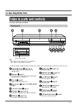

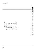


Index to parts and controls (Continued)
Rear panel
1
2
3
4
6
7
8
9
5
5 COMPONENT OUT jacks
page 17 in
“INSTALLATION GUIDE”
Outputs video signals to a connected TV or
monitor.
Connects to a TV or monitor equipped with
component video jacks.
6 AV2(EXT) socket
page 39
Use this socket when connecting the video or
other equipment that has the terminal in this
shape.
7 VHF/UHF RF IN (FROM ANT.) input socket
page 14 in “INSTALLATION GUIDE”
Connects to an aerial or satellite signal.
1 Power cord
page 15 in “INSTALLATION
GUIDE”
Connects to a wall outlet.
2 Ventilation fan
3 DIGITAL AUDIO OUT COAXIAL jack
page 20
in “INSTALLATION GUIDE”
Use this to connect the recorder to an audio
receiver equipped with a coaxial digital audio input
jack.
4 AV OUT 1, AV OUT 2 jacks
page 16 in
“INSTALLATION GUIDE”
Outputs video and audio signals to a connected
TV or amplifier.
Operating Instructions
12-3
Summary of Contents for RD-XS24SB
Page 10: ...Product Specification 2 4 MEMO ...
Page 12: ...3 2 Software Update MEMO ...
Page 20: ...4 8 Disassembly and Reaasembly MEMO ...
Page 34: ...Troubleshooting 5 14 MEMO ...
Page 35: ...6 1 6 Exploded View and Parts List 6 1 Cabinet Assembly Page 6 2 ...
Page 38: ...Exploded Views and Parts List 6 4 MEMO ...
Page 50: ...Electrical Parts List 7 12 MEMO ...
Page 160: ...Operating Instructions 12 110 MEMO ...
Page 173: ...1 1 SHIBAURA 1 CHOME MINATO KU TOKYO 105 8001 JAPAN ...
Page 177: ...Block Diagrams 8 3 8 2 Digital Block Diagram ...
Page 180: ...Block Diagrams 8 6 8 5 AIC01 MSP3417 Block Diagram ...
Page 181: ...Block Diagrams 8 7 8 6 AIC02 AIC07 MC14052 Block Diagram ...
Page 182: ...Block Diagrams 8 8 8 7 AIC03 AK5357 Block Diagram ...
Page 183: ...Block Diagrams 8 9 8 8 AIC04 PCM1753 Block Diagram ...
Page 184: ...Block Diagrams 8 10 8 9 KIC01 PT6961 Block Diagram ...
Page 185: ...Block Diagrams 8 11 8 10 MIC01 78F4225 Block Diagram ...
Page 187: ...Block Diagrams 8 13 8 12 SIC01 MM1647 Block Diagram ...
Page 188: ...Block Diagrams 8 14 8 13 VIC01 74HC4051 Block Diagram ...
Page 189: ...Block Diagrams 8 15 8 14 VIC05 MM1568 Block Diagram ...
Page 190: ...Block Diagrams 8 16 MEMO ...
Page 191: ...9 Wiring Diagram 9 1 ...
Page 192: ...Wiring Diagram 9 2 MEMO ...
Page 194: ...PCB Diagrams 10 2 10 1 S M P S PCB COMPONENT SIDE ...
Page 195: ...PCB Diagrams 10 3 CONDUCTOR SIDE ...
Page 196: ...PCB Diagrams 10 4 10 2 Main PCB COMPONENT SIDE ...
Page 198: ...PCB Diagrams 10 6 10 3 Jack PCB COMPONENT SIDE ...
Page 199: ...PCB Diagrams 10 7 CONDUCTOR SIDE ...
Page 200: ...PCB Diagrams 10 8 10 4 Key PCB COMPONENT SIDE CONDUCTOR SIDE ...
Page 202: ...Schematic Diagrams 11 2 11 1 S M P S SMPS PCB ...
Page 203: ...Schematic Diagrams 11 3 11 2 Main Main PCB ...
Page 204: ...Schematic Diagrams 11 4 11 3 Audio Jack PCB ...
Page 205: ...Schematic Diagrams 11 5 11 4 Video Jack PCB ...
Page 206: ...Schematic Diagrams 11 6 11 5 AV switch Scart Jack PCB ...
Page 207: ...Schematic Diagrams 11 7 11 6 Tuner Front in Connection Jack PCB ...
Page 208: ...Schematic Diagrams 11 8 11 7 Micom Jack PCB ...
Page 209: ...Schematic Diagrams 11 9 11 8 Key Key PCB ...
Page 210: ...Schematic Diagrams 11 10 MEMO ...


