


3-1
3. Software Update
1) Introduction
Toshiba will often support software update to improve the performance of DVD Recorder to the latest status.
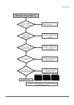
2) How to make Main-Board(Back-end)
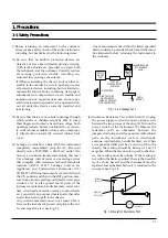
!
Power on.
@
Disc tray open.
#
Insert update CD.
$
Tray close. Set loads update-data in CD.
When update is starting normally, LED-display displays "V-UP".
%
Wait until update is finished. After update is finished, LED-display displays "MP" for a moment.
And opening tray, set turns stand-by mode automatically.
It is very important : please read the below notice before updating your unit.
The following events may interrupt the update process and MAY RESULT IN PERMANENT DAMAGE TO THE
UNIT WHILE UPDATING
!
The power cord unplugged.
@
Power Outage.
#
Dirt or Scratches on the disc.
$
Opening a disc tray during processing.
Caution
Summary of Contents for RD-XS24SB
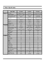
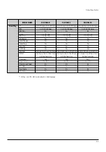
Page 10: ...Product Specification 2 4 MEMO ...
Page 12: ...3 2 Software Update MEMO ...
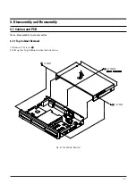
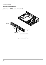
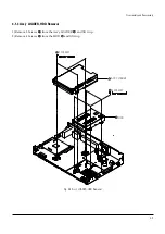
Page 20: ...4 8 Disassembly and Reaasembly MEMO ...
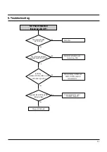
Page 34: ...Troubleshooting 5 14 MEMO ...
Page 35: ...6 1 6 Exploded View and Parts List 6 1 Cabinet Assembly Page 6 2 ...
Page 38: ...Exploded Views and Parts List 6 4 MEMO ...
Page 50: ...Electrical Parts List 7 12 MEMO ...
Page 160: ...Operating Instructions 12 110 MEMO ...
Page 173: ...1 1 SHIBAURA 1 CHOME MINATO KU TOKYO 105 8001 JAPAN ...
Page 177: ...Block Diagrams 8 3 8 2 Digital Block Diagram ...
Page 180: ...Block Diagrams 8 6 8 5 AIC01 MSP3417 Block Diagram ...
Page 181: ...Block Diagrams 8 7 8 6 AIC02 AIC07 MC14052 Block Diagram ...
Page 182: ...Block Diagrams 8 8 8 7 AIC03 AK5357 Block Diagram ...
Page 183: ...Block Diagrams 8 9 8 8 AIC04 PCM1753 Block Diagram ...
Page 184: ...Block Diagrams 8 10 8 9 KIC01 PT6961 Block Diagram ...
Page 185: ...Block Diagrams 8 11 8 10 MIC01 78F4225 Block Diagram ...
Page 187: ...Block Diagrams 8 13 8 12 SIC01 MM1647 Block Diagram ...
Page 188: ...Block Diagrams 8 14 8 13 VIC01 74HC4051 Block Diagram ...
Page 189: ...Block Diagrams 8 15 8 14 VIC05 MM1568 Block Diagram ...
Page 190: ...Block Diagrams 8 16 MEMO ...
Page 191: ...9 Wiring Diagram 9 1 ...
Page 192: ...Wiring Diagram 9 2 MEMO ...
Page 194: ...PCB Diagrams 10 2 10 1 S M P S PCB COMPONENT SIDE ...
Page 195: ...PCB Diagrams 10 3 CONDUCTOR SIDE ...
Page 196: ...PCB Diagrams 10 4 10 2 Main PCB COMPONENT SIDE ...
Page 198: ...PCB Diagrams 10 6 10 3 Jack PCB COMPONENT SIDE ...
Page 199: ...PCB Diagrams 10 7 CONDUCTOR SIDE ...
Page 200: ...PCB Diagrams 10 8 10 4 Key PCB COMPONENT SIDE CONDUCTOR SIDE ...
Page 202: ...Schematic Diagrams 11 2 11 1 S M P S SMPS PCB ...
Page 203: ...Schematic Diagrams 11 3 11 2 Main Main PCB ...
Page 204: ...Schematic Diagrams 11 4 11 3 Audio Jack PCB ...
Page 205: ...Schematic Diagrams 11 5 11 4 Video Jack PCB ...
Page 206: ...Schematic Diagrams 11 6 11 5 AV switch Scart Jack PCB ...
Page 207: ...Schematic Diagrams 11 7 11 6 Tuner Front in Connection Jack PCB ...
Page 208: ...Schematic Diagrams 11 8 11 7 Micom Jack PCB ...
Page 209: ...Schematic Diagrams 11 9 11 8 Key Key PCB ...
Page 210: ...Schematic Diagrams 11 10 MEMO ...


