


Operating Instructions
12-106
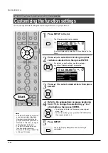
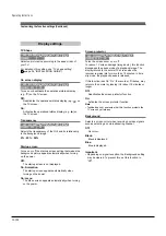
Customizing the function settings (Continued)
DVD recorder operation
AV record quality
HDD
DVD-RAM
DVD-RW
(VR)
DVD-RW
(Video)
DVD-R
(VR)
DVD-VIDEO
VCD
CD
DVD-R
(Video)
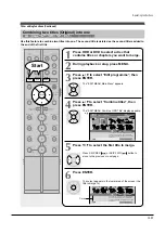
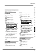
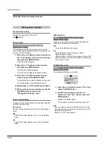
You can select from 4 combined picture and sound
quality recording settings prior to actual recording.
Actual selection applied becomes the default setting for
the normal recording or programmed recording.
Sound and picture quality for the three recording settings
of XP, SP and LP cannot be altered. You can freely
change the settings by using “Manual mode set”.
Set in advance frequently used recording settings for
DVD or HDD.
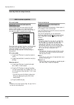
AV record quality
1) Press the / buttons to select the media to
record.
2) Press the / buttons to select the recording
settings.
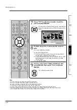
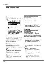
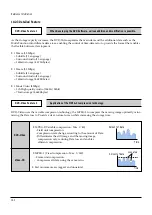
Manual mode set.
1) Press the / buttons to select the desired
item, “Rate” or “Audio quality”.
2) Press the / buttons to change the setting.
You can adjust “Rate” by 0.2 Mbps from 1.0 to
9.2. (You cannot set the rate from 1.0 to 1.4 and
1.4 to 2.0.)
• If you set the rate of the “Rate” setting to 9.2,
XP may be displayed in spite of the Audio
quality setting.
3) Press the ENTER button.
Note
• Depending on the sound quality settings, the upper limit for
the picture quality setting differs.
Picture record mode
HDD
DVD-RAM
DVD-RW
(VR)
DVD-RW
(Video)
DVD-R
(VR)
DVD-VIDEO
VCD
CD
DVD-R
(Video)
Adjusts problems with the brightness of video signals of
TV broadcasts or other external input.
Press the
/ buttons to select the source, and the /
buttons to select the mode.
(Only use this setting when you cannot adjust the
brightness satisfactorily with the “Custom picture setting”
in the “Picture/Audio settings” (
Page 118) of this
recorder.)
Important:
• This setting changes the video signal to record and the
recorded signal is not returned to the original state even
when this setting is changed after recording. When
duplicating from VHS tape, if you can check the video
recording state beforehand, we recommend first playing
back for a while and checking the overall brightness
tendency, then setting an appropriate mode.
Standard:
The brightness of signals received with this recorder
and external input signals is adjusted automatically.
Use this mode normally.
Mode 1:
This setting is used to record the signals darker when
the screen is too bright.
Mode 2, 3, 4:
As the number rises, the signals are recorded brighter.
Use these modes to adjust the brightness.
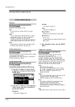
AV record quality
Manual mode set.
Total recording time: approx.
61min.
(with 4.7 GB unused)
9.2
XP
4.6
D/M1
D/M1
Rate
9.2
Audio quality
D/M1
HDD rec
DVD rec
SP
e.g.
Summary of Contents for RD-XS24SB
Page 10: ...Product Specification 2 4 MEMO ...
Page 12: ...3 2 Software Update MEMO ...
Page 20: ...4 8 Disassembly and Reaasembly MEMO ...
Page 34: ...Troubleshooting 5 14 MEMO ...
Page 35: ...6 1 6 Exploded View and Parts List 6 1 Cabinet Assembly Page 6 2 ...
Page 38: ...Exploded Views and Parts List 6 4 MEMO ...
Page 50: ...Electrical Parts List 7 12 MEMO ...
Page 160: ...Operating Instructions 12 110 MEMO ...
Page 173: ...1 1 SHIBAURA 1 CHOME MINATO KU TOKYO 105 8001 JAPAN ...
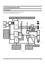
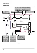
Page 177: ...Block Diagrams 8 3 8 2 Digital Block Diagram ...
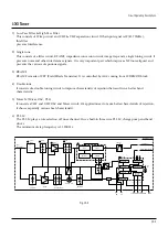
Page 180: ...Block Diagrams 8 6 8 5 AIC01 MSP3417 Block Diagram ...
Page 181: ...Block Diagrams 8 7 8 6 AIC02 AIC07 MC14052 Block Diagram ...
Page 182: ...Block Diagrams 8 8 8 7 AIC03 AK5357 Block Diagram ...
Page 183: ...Block Diagrams 8 9 8 8 AIC04 PCM1753 Block Diagram ...
Page 184: ...Block Diagrams 8 10 8 9 KIC01 PT6961 Block Diagram ...
Page 185: ...Block Diagrams 8 11 8 10 MIC01 78F4225 Block Diagram ...
Page 187: ...Block Diagrams 8 13 8 12 SIC01 MM1647 Block Diagram ...
Page 188: ...Block Diagrams 8 14 8 13 VIC01 74HC4051 Block Diagram ...
Page 189: ...Block Diagrams 8 15 8 14 VIC05 MM1568 Block Diagram ...
Page 190: ...Block Diagrams 8 16 MEMO ...
Page 191: ...9 Wiring Diagram 9 1 ...
Page 192: ...Wiring Diagram 9 2 MEMO ...
Page 194: ...PCB Diagrams 10 2 10 1 S M P S PCB COMPONENT SIDE ...
Page 195: ...PCB Diagrams 10 3 CONDUCTOR SIDE ...
Page 196: ...PCB Diagrams 10 4 10 2 Main PCB COMPONENT SIDE ...
Page 198: ...PCB Diagrams 10 6 10 3 Jack PCB COMPONENT SIDE ...
Page 199: ...PCB Diagrams 10 7 CONDUCTOR SIDE ...
Page 200: ...PCB Diagrams 10 8 10 4 Key PCB COMPONENT SIDE CONDUCTOR SIDE ...
Page 202: ...Schematic Diagrams 11 2 11 1 S M P S SMPS PCB ...
Page 203: ...Schematic Diagrams 11 3 11 2 Main Main PCB ...
Page 204: ...Schematic Diagrams 11 4 11 3 Audio Jack PCB ...
Page 205: ...Schematic Diagrams 11 5 11 4 Video Jack PCB ...
Page 206: ...Schematic Diagrams 11 6 11 5 AV switch Scart Jack PCB ...
Page 207: ...Schematic Diagrams 11 7 11 6 Tuner Front in Connection Jack PCB ...
Page 208: ...Schematic Diagrams 11 8 11 7 Micom Jack PCB ...
Page 209: ...Schematic Diagrams 11 9 11 8 Key Key PCB ...
Page 210: ...Schematic Diagrams 11 10 MEMO ...


