


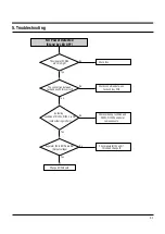

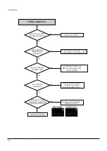

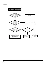


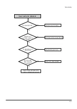
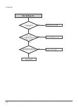


Troubleshooting
5-6
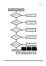
1 pin and 5 pin in CON03 of
jack PCB has normal
level?
Analog signal are
Inputted normally
5pin of SIC05
Analog signal are
out normally
SIC01-29(AV2),30(AV1)
Check the connection between
SIC01 and SCART Jack
-AV1 ; 30 pin of SIC02 and 19 pin of AV1
-AV2 : 29 pin of SIC02 and 40 pin of AV2
Check Main PCB
No
No
Check the connection between 1 pin
and 5 pin of CON03 in Jack PCB and SIC01
No
Check the I2C lin2
(between SIC01-32, 33
and MIC01(Pin 16,18)
Check the SMPS
(AL5.8V)
Yes
Yes
Yes
Check the power
supply to 2, 4, 6pin of SIC01?
No
Yes
AV1, AV2 (CVBS) output error
Summary of Contents for RD-XS24SB
Page 10: ...Product Specification 2 4 MEMO ...
Page 12: ...3 2 Software Update MEMO ...
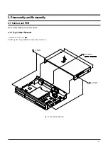
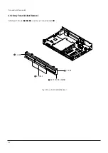
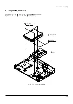
Page 20: ...4 8 Disassembly and Reaasembly MEMO ...
Page 34: ...Troubleshooting 5 14 MEMO ...
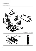
Page 35: ...6 1 6 Exploded View and Parts List 6 1 Cabinet Assembly Page 6 2 ...
Page 38: ...Exploded Views and Parts List 6 4 MEMO ...
Page 50: ...Electrical Parts List 7 12 MEMO ...
Page 160: ...Operating Instructions 12 110 MEMO ...
Page 173: ...1 1 SHIBAURA 1 CHOME MINATO KU TOKYO 105 8001 JAPAN ...
Page 177: ...Block Diagrams 8 3 8 2 Digital Block Diagram ...
Page 180: ...Block Diagrams 8 6 8 5 AIC01 MSP3417 Block Diagram ...
Page 181: ...Block Diagrams 8 7 8 6 AIC02 AIC07 MC14052 Block Diagram ...
Page 182: ...Block Diagrams 8 8 8 7 AIC03 AK5357 Block Diagram ...
Page 183: ...Block Diagrams 8 9 8 8 AIC04 PCM1753 Block Diagram ...
Page 184: ...Block Diagrams 8 10 8 9 KIC01 PT6961 Block Diagram ...
Page 185: ...Block Diagrams 8 11 8 10 MIC01 78F4225 Block Diagram ...
Page 187: ...Block Diagrams 8 13 8 12 SIC01 MM1647 Block Diagram ...
Page 188: ...Block Diagrams 8 14 8 13 VIC01 74HC4051 Block Diagram ...
Page 189: ...Block Diagrams 8 15 8 14 VIC05 MM1568 Block Diagram ...
Page 190: ...Block Diagrams 8 16 MEMO ...
Page 191: ...9 Wiring Diagram 9 1 ...
Page 192: ...Wiring Diagram 9 2 MEMO ...
Page 194: ...PCB Diagrams 10 2 10 1 S M P S PCB COMPONENT SIDE ...
Page 195: ...PCB Diagrams 10 3 CONDUCTOR SIDE ...
Page 196: ...PCB Diagrams 10 4 10 2 Main PCB COMPONENT SIDE ...
Page 198: ...PCB Diagrams 10 6 10 3 Jack PCB COMPONENT SIDE ...
Page 199: ...PCB Diagrams 10 7 CONDUCTOR SIDE ...
Page 200: ...PCB Diagrams 10 8 10 4 Key PCB COMPONENT SIDE CONDUCTOR SIDE ...
Page 202: ...Schematic Diagrams 11 2 11 1 S M P S SMPS PCB ...
Page 203: ...Schematic Diagrams 11 3 11 2 Main Main PCB ...
Page 204: ...Schematic Diagrams 11 4 11 3 Audio Jack PCB ...
Page 205: ...Schematic Diagrams 11 5 11 4 Video Jack PCB ...
Page 206: ...Schematic Diagrams 11 6 11 5 AV switch Scart Jack PCB ...
Page 207: ...Schematic Diagrams 11 7 11 6 Tuner Front in Connection Jack PCB ...
Page 208: ...Schematic Diagrams 11 8 11 7 Micom Jack PCB ...
Page 209: ...Schematic Diagrams 11 9 11 8 Key Key PCB ...
Page 210: ...Schematic Diagrams 11 10 MEMO ...


