Design Files
76
JAJU324B – March 2015 – Revised July 2017
翻訳版
—
最新の英語版資料
http://www-s.ti.com/sc/techlit/TIDU832
Copyright © 2015–2017, Texas Instruments Incorporated
EMI/EMC
規格準拠、産業用温度範囲のデュアルポート・ギガビット・イーサネットの
リファレンス・デザイン
6
Design Files
6.1
Schematics
To download the schematics, see the design files at
.
6.2
Bill of Materials
To download the bill of materials (BOM), see the design files at
6.3
Layer Plots
To download the layer plots, see the design files at
.
6.4
PCB Layout Guidelines
6.4.1
Layer Stack
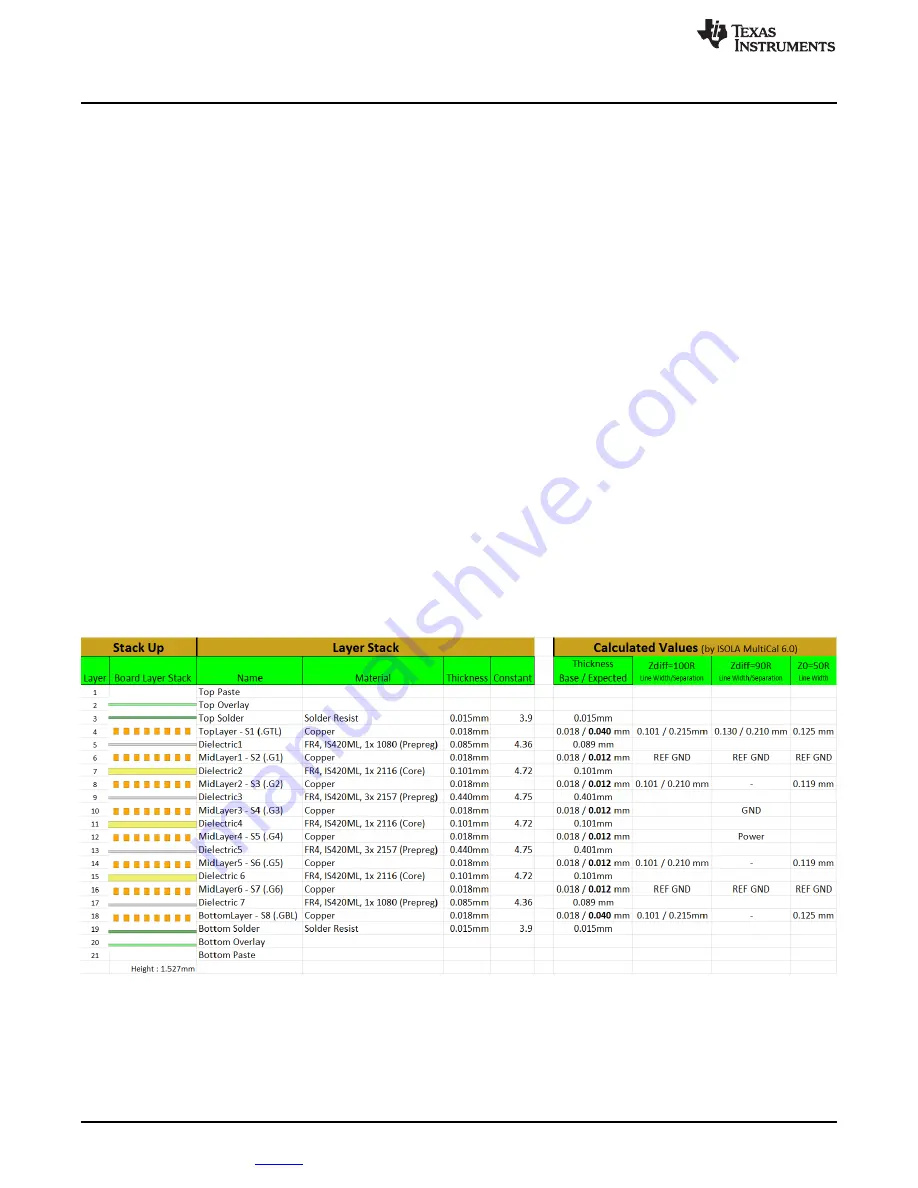
Ensure that the differential signal layers have a reference ground and that the PCB differential signal
traces are matched to 100-
Ω
impedance. For the single-ended traces, the board is matched to 50
Ω
.
A layer size of 0.018 mm was chosen for the top and mid layers. This size can be defined as the base
thickness. When actually building the board, the mid layers will decrease in size and the outer layers will
increase in size. This means that the expected top layer thickness would be 0.040 mm and a mid layer
would have an expected thickness of 0.012 mm. This decrease and increase in thickness varies on the
manufacturer. This variation is why it is very important when working with high-speed differential signals to
define the layer stack and double check with the PCB manufacturer to ensure that the expected
impedances are achieved.
図
図
70. Layer Stack
For a less complex processor design, the PCB layers for DP83867IR routing can be reduced to four
layers. See the DP83867IR data sheet for examples


