


xE922-3GR Hardware User Guide
1VV0301272
Rev.0.8 2017-01-05
Reproduction forbidden without written authorization from Telit Communications S.p.A. - All Rights
Reserved.
Page 81 of 112
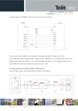
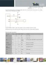
14.
Debug / flash interfaces
For debugging and/or flashing FW to the xE922-3GR module, several interfaces are available.
Please refer to EVB documentation for example of debug connector implementations.
14.1.
USB2.0 HS
This interface can be used as image flash download and debug interface (ADB debug interface)
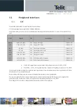
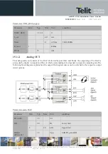
14.2.
USIF2
UART configuration, can be used for SW logging UART.
An UART-USB convertor could be attached to connect to PC USB port directly).
By default USIF2 is configured for this logging UART interface, but alternatively USIF1 as well could be
used.
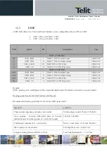
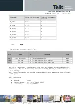
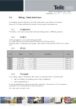
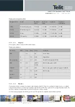
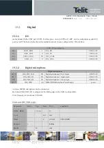
14.3.
JTAG
PAD
Signal
I/O
descriptions
Type
AT4
JTAG_TDO
O
JTAG
CMOS 1.8V
AN4
JTAG_TDI
I
JTAG
CMOS 1.8V
AR4
JTAG_TMS
I
JTAG
CMOS 1.8V
AV4
JTAG_TCK
O
JTAG
CMOS 1.8V
AW5
JTAG_TRST
O
JTAG
CMOS 1.8V
AW3
JTAG_RTCK
I
JTAG
CMOS 1.8V
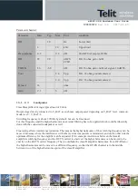
14.4.
Test pads
For test/debug
purpose, the following ‘RFU’ pins are recomme
nded to have test pads attached:
·
AB19: SoC RESET_IN (internally driven by PMU AGOLD620)
·
AD19: SoC RESET_OUT
In case the application main board, because of place restrictions, cannot foresee in a JTAG connector
placeholder, it is recommended to attach at least test pads on:
AT4, AN4, AR4, AV4, AW5, AW3