


xE922-3GR Hardware User Guide
1VV0301272
Rev.0.8 2017-01-05
Reproduction forbidden without written authorization from Telit Communications S.p.A. - All Rights
Reserved.
Page 62 of 112
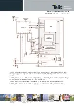
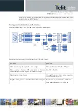
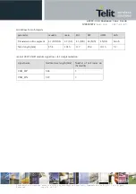
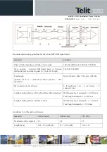
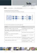
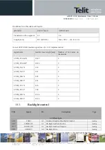
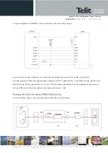
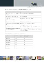
Actual xE922-3GR module signal trace (L1+L2) implementation:
signal name
module trace length [mm]
Number of microvias on
the module
DSI_CLKN
9.88
2
DSI_CLKP
9.65
2
DSI_DN0
7.39
2
DSI_DP0
7.15
2
DSI_DN1
9.09
2
DSI_DP1
9.28
2
DSI_DN2
8.60
2
DSI_DP2
8.43
2
DSI_DN3
12.16
2
DSI_DP3
12.01
2
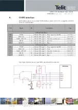
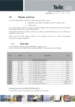
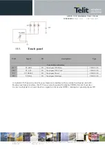
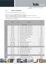
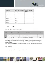
10.2.
LVDS
4-
lane ‘Low voltage differential signaling’
LVDS transmitter, implementing the LVDS PHY with electrical
parameters according TIA/EIA-644 technical standard.
LVDS Clock range: 20
–
170 MHz.
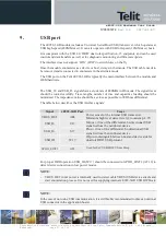
PAD
Signal
I/O
descriptions
Type
LVDS Display Interface
W19
LVDS_TA1P
AO
LVDS Data A Positive
Analog
U19
LVDS_TA1N
AO
LVDS Data A Negative
Analog
X18
LVDS_TB1P
AO
LVDS Data B Positive
Analog
V18
LVDS_TB1N
AO
LVDS Data B Negative
Analog
V20
LVDS_TC1P
AO
LVDS Data C Positive
Analog
T20
LVDS_TC1N
AO
LVDS Data C Negative
Analog
Y21
LVDS_TD1P
AO
LVDS Data D Positive
Analog
W21
LVDS_TD1N
AO
LVDS Data D Negative
Analog
U21
LVDS_TCLK1P
AO
LVDS Clock Positive
Analog