


xE922-3GR Hardware User Guide
1VV0301272
Rev.0.8 2017-01-05
Reproduction forbidden without written authorization from Telit Communications S.p.A. - All Rights
Reserved.
Page 79 of 112
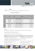
Each SoC
pad’s characteristics are controlled by a peripheral called PCL (Port Control Logic
).
In the next page table a
‘
complete
’
overview of all PCL muxing options for
‘
all DBB pins externally
available
’
on the xE922-3GR module LGA pinout is detailed out.
In order to clarify the correspondence between the module’s pin naming and chip set supplier docume
ntation
naming convention, the DBB SoC BGA ball pin /signal names as well as xE922-3GR LGA pin number /
signal names are indicated in different columns.
Yellow color code highlights the xE922-3GR
module’s
intentional target use.
Note:
Please
note GPIO2_EINT4 is applicable as “input only” because of internal level shift circuitry to
accommodate for 5V VBUS_USB level detect.
Please consult Intel Business Link Support (IBL) for detailed info (like SW user guide) how to program the
GPIO configuration/multiplex for your specific application.
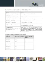
Each pad has following characteristics indicated:
Pad pull class:
This is the pull-up and pull-down strength of the pad that can be enabled/disabled using PCL
registers. There are three pull classes of pads on 1.8V IO domain, A, B, and D (C is not used). A is the
strongest (PU=155uA typ, PD=135uA Typ), B is medium (PU=80.8uA typ, PD=64uA typ) and D is the
weakest (PU=16.4uA typ, PD=16.2uA typ). Pull-up/pull-down can be enabled through PCL registers but their
strength is fixed as indicated in the GPIO spreadsheet, refer to it for each individual pad’s pull class.
Drive strength
, also referred to as drive/output current for the pad. 2mA, 4mA, 8mA and 12mA are supported
and can be selected by PCL register.
Buffer Type:
Schmitt Trigger ST or buffer BU. This setting is not selectable through PCL registers. Refer to
GPIO spreadsheet for each individual pad’s buffer type.
RESET state during RESET (PU or PD):
All pads come up in a default state during and after reset until
PCL registers are initialized. It is important to note that connection of each GPIO to application circuit
requires determination whether application circuit is sensitive to the GPIO being HIGH or LOW at reset, e.g.,
it might not be desirable to have an RF transmitter enabled by default during power-on reset so the GPIO
allocated to its RESET and/or power-
down input should be such that it holds the transmitter in “disabled”
state at the time of power-on until SW takes control. Refer to GPIO table
for each individual pad’s default
state at reset.
Signal direction during RESET (input or output):
Refer to GPIO table
for each individual pad’s default
direction at reset.
Functions multiplexed on each pad:
Each pad not associated with dedicated interfaces can have up to 7
alternate functions multiplexed on it in addition to GPIO function. Refer to GPIO table for each individual
pad’s alternate functions.
Interrupts: the chip set supports sixteen external interrupts (EINT[15:0]) signals that are multiplexed on
different pins but can only be used in one location. Not all interrupt signals are available as some are on pins
used for dedicated functions.
GPIOs and their different aspects described above can be configured through SW. Please refer to software
architecture document for more details.