


xE922-3GR Hardware User Guide
1VV0301272
Rev.0.8 2017-01-05
Reproduction forbidden without written authorization from Telit Communications S.p.A. - All Rights
Reserved.
Page 63 of 112
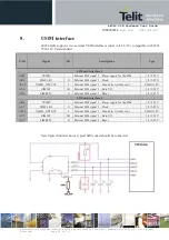
S21
LVDS_TCLK1N
AO
LVDS Clock Negative
Analog
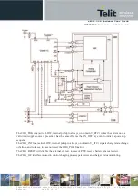
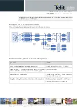
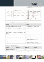
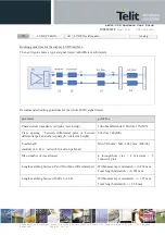
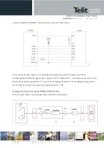
Routing guide lines for the display LVDS interface:
The next figure shows a typical signal traject with different sub trajects.
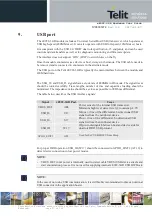
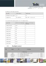
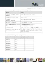
Recommended routing guidelines for the whole LVDS signal traject:
parameter
guideline
Characteristic impedance (stripline / microstrip)
100 ohm differential 10%(SL) 15%(MS)
Trace spacing : between differential pairs or between
differential pair and other signals (h = dielectric height)
5xh (SL) 7xh (MS)
Total length
(module (L1+L2) + carrier(L3)+add-on pcb(L4))
Min. 50.8 mm / Max. 203.2 mm (MS/SL)
Max. number of vias allowed
4 through-hole vias + 4 microvias + 2
connector pins
Length matching between P and N within a differential pair
Within same layer mismatch: +/-0.254 mm
Total length mismatch: +/-0.381 mm
Length matching between DATA to CLK
Within same layer mismatch : +/- 1.27 mm
Total length mismatch: +/- 2.54 mm