— 72 —
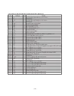
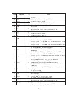
Pin Name
PDCLK
V
SS
VSYNC
HSYNC
SO
FID
V
DD
XIICEN
Pin No.
57
58
59
60
61
62
63
64
I/O
O
–
O
O
O
O
–
O
Function
13.5MHz pixel data clock output pin.
This clock is obtained by 1/2 frequency-dividing SYSCLK.
Used only in the 16-bit pixel data mode.
Digital ground
V.sync signal output
H.sync signal output
The functions of this pin are selected by Pin 64 XIICEN.
When the XIICEN pin is “H”, sets into the SONY SIO mode, and becomes the S0 serial-
out output pin.
When the XIICEN pin is “L”, this pin is not used and sets into high impedance.
Field ID output.
When control register bit “FDS”=“1”, “L” indicates the first field and “H” indicates the
second field.
When control register bit “FDS”=“0”, “H” indicates the first field and “L” indicates the
second field.
Digital power supply
Serial interface mode selection input pin. Pulled-up.
When “L”, Pins 48 to 50, and 61 set into the I
2
C-BUS mode.
When “H”, Pins 48 to 50, and 61 set into the SONY SOP mode.
Summary of Contents for MCE-K700
Page 8: ... 8 ...
Page 9: ... 9 ...
Page 10: ... 10 ...
Page 11: ... 11 ...
Page 12: ... 12 ...
Page 13: ... 13 ...
Page 14: ... 14 ...
Page 15: ... 15 ...
Page 16: ... 16 ...
Page 21: ......
Page 22: ......
Page 23: ......
Page 24: ......
Page 25: ......
Page 26: ......
Page 27: ......

