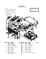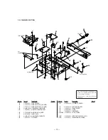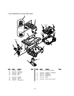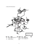
— 64 —
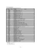
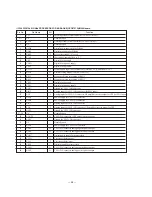
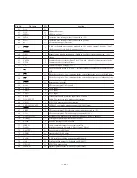
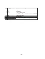
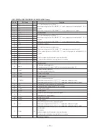
I/O
I/O
I/O
I/O
–
–
I/O
I/O
I/O
I/O
I/O
I/O
I/O
I/O
I/O
I/O
I
I
I
I
–
–
I
O
O
O
O
O
O
O
O
O
O
O
–
–
O
O
O
O
O
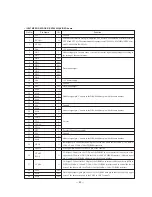
Function
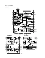
Data input/output signal pin. Connect to the DRAM data pin so that the lower and upper
bytes of the data correspond to the CAS0 to CAS3 controls.
+5V power supply
Ground
Data input/output signal pin. Connect to the DRAM data pin so that the lower and upper
bytes of the data correspond to the CAS0 to CAS3 controls.
OSD enable signal
OSD data input pin. When the XOSDEN input is L, the color registered in the register
specified by this 3 inputs (3 bits) is output as the image data. (Connected to ground)
+5V power supply
Ground
Video output enable signal pin. When set to ‘L’, enables the image data output and DCLK
output. When set to ‘H’, disables (high impedance). Output control can also be performed
by writing in the register.
Output pin of the R or Cr signal of the image data. MSB is R/Cr7. Synchronizes with
DCLK.
Output pin of the G or Y signal of the image data. MSB is G/Y7. Synchronizes with DCLK.
+5V power supply
Ground
Output pin of the G or Y signal of the image data. MSB is G/Y7. Synchronizes with DCLK.
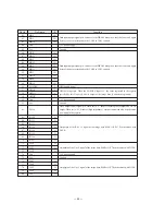
Pin Name
MD9
MD5
MD10
V
DD
V
SS
MD4
MD11
MD3
MD12
MD2
MD13
MD1
MD14
MD0
MD15
XOSDEN
OSDB
OSDG
OSDR
V
DD
V
SS
XVOE
R/Cr0
R/Cr1
R/Cr2
R/Cr3
R/Cr4
R/Cr5
R/Cr6
R/Cr7
G/Y0
G/Y1
G/Y2
V
DD
V
SS
G/Y3
G/Y4
G/Y5
G/Y6
G/Y7
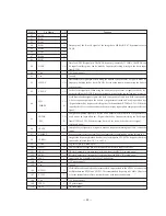
Pin No.
41
42
43
44
45
46
47
48
49
50
51
52
53
54
55
56
57
58
59
60
61
62
63
64
65
66
67
68
69
70
71
72
73
74
75
76
77
78
79
80
Summary of Contents for MCE-K700
Page 8: ... 8 ...
Page 9: ... 9 ...
Page 10: ... 10 ...
Page 11: ... 11 ...
Page 12: ... 12 ...
Page 13: ... 13 ...
Page 14: ... 14 ...
Page 15: ... 15 ...
Page 16: ... 16 ...
Page 21: ......
Page 22: ......
Page 23: ......
Page 24: ......
Page 25: ......
Page 26: ......
Page 27: ......

