— 71 —
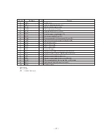
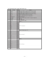
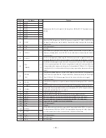
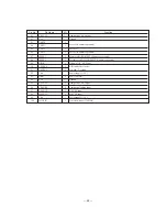
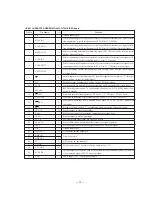
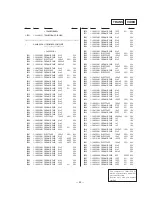
Pin Name
TD9
TD8
XTEST1
XTEST2
XTEST3
V
SS
TRST
V
DD
TDI
TMS
TCK
TDO
V
SS
SI
SCK
XCS
XVRST
F1
V
DD
XTEST4
XRST
SYSCLK
Pin No.
35
36
37
38
39
40
41
42
43
44
45
46
47
48
49
50
51
52
53
54
55
56
I/O
I/O
I/O
I
I
I
–
I
–
I
I
I
O
–
I
I
I
I
I
–
I
I
I
Function
Test data bus.
Set to open.
In the test mode, used for internal circuit test data bus.
The test mode is allowed to use only for device vendors.
Test mode control input pin. Pulled-up.
When these pins are “H”, CXD1913Q is not in the test mode.
The test mode is allowed to use only for device vendors.
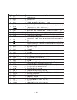
Digital ground
Test mode reset input pin.
During power on/reset, set to “L” for more than 40 clocks (SYSCLK).
Digital power supply.
Test mode control input pin. Pulled-up.
Test mode control input pin. Fix at “H”.
Test data bus pin. Set to open.
Digital ground
The functions of this pin are selected by Pin 64 XIICEN.
When the XIICEN pin is “H”, sets into the SONY SIO mode, and becomes the SI serial
data input pin.
When the XIICEN pin is “L”, sets into the I
2
C-BUS mode, and becomes the SDA input/
output pin.
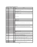
The functions of this pin are selected by Pin 64 XIICEN.
When the XIICEN pin is “H”, sets into the SONY SIO mode, and becomes the SCK serial
clock input pin.
When the XIICEN pin is “L”, sets into the I
2
C-BUS mode, and becomes the SCL input pin.
The functions of this pin are selected by Pin 64 XIICEN. Pulled-up.
When the XIICEN pin is “H”, sets into the SONY SIO mode, and becomes the XCK chip
select input pin.
When the XIICEN pin is “L”, sets into the I
2
C-BUS mode, and becomes the SA slave
address selection input signal which selects the I
2
C-BUS slave address.
Active “L” vertical sync reset input pin. Pulled-up.
Used for synchronizing external vertical sync and internal vertical sync.
When XVRST is “L”, the internal digital sync generator is reset according to the F1 state.
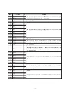
Field ID input pin.
When externally synchronizing with the XVRST signal, the field to be reset is determined
by this signal.
“H” indicates the first field.
“L” indicates the second field.
Digital power supply
Test mode control input pin. Pulled-up.
When these pins are “H”, CXD1913Q is not s test mode.
The test mode is allowed to use only for device vendors.
System reset input pin when active “L”.
During power on/reset, set to “L” for more than 40 clocks (SYSCLK).
System clock input pin.
To generate the correct sub carrier frequency, precisely 27MHz is required.
Summary of Contents for MCE-K700
Page 8: ... 8 ...
Page 9: ... 9 ...
Page 10: ... 10 ...
Page 11: ... 11 ...
Page 12: ... 12 ...
Page 13: ... 13 ...
Page 14: ... 14 ...
Page 15: ... 15 ...
Page 16: ... 16 ...
Page 21: ......
Page 22: ......
Page 23: ......
Page 24: ......
Page 25: ......
Page 26: ......
Page 27: ......

