— 65 —
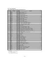
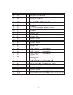
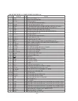
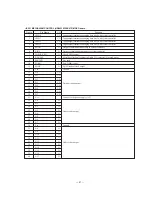
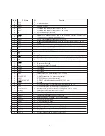
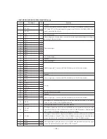
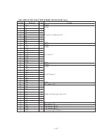
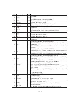
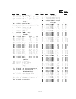
Pin Name
B/Cb0
B/Cb1
B/Cb2
B/Cb3
B/Cb4
B/Cb5
B/Cb6
B/Cb7
DCLK
V
DD
V
SS
HSYNC
VSYNC
FID
/FHREF
CBLNK
/FSC
CSYNC
XSGRST
CLK0O
DOUT
DATO
LRCO
BCKO
FSXI
V
DD
V
SS
XTL2O
XTL2I
V
DD
C2PO
LRCI
Pin No.
81
82
83
84
85
86
87
88
89
90
91
92
93
94
95
96
97
98
99
100
101
102
103
104
105
106
107
108
109
110
I/O
O
O
O
O
O
O
O
O
I/O
–
–
I/O
I/O
I/O
/O
I/O
/O
O
I
O
O
O
O
O
I
–
–
O
I
–
I
I
Function
Output pin of the B or Cb signal of the image data. MSB is B/Cb7. Synchronizes with
DCLK.
Dot clock (DCLK) signal pin. The DCLK frequency is normally 13.5MHz. The DCLK can
be input from this pin or can be made by frequency-dividing (1/integer) the clock input
from XTL0I.
+5V power supply
Ground
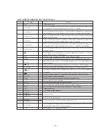
Horizontal sync signal pin. When using the built-in sync generator, a signal is made by
frequency-dividing the dot clock (DCLK). Serves as the input when not using the built-in
sync generator.
Vertical sync signal pin. When using the built-in sync generator, a signal is made by fre-
quency-dividing the DCLK. Serves as the input when not using the built-in sync generator.
Field determination signal signal. Odd field correspond to H and even field correspond to
L. Serves as an output when the built-in sync generator is used, and as an input when not.
/ Signal obtained by frequency-dividing the clock input from XTL0I or XTLI. When the
input clock is 8 fsc, it can be used as the horizontal sync signal phase comparison reference
signal.
Composite blanking signal pin. Serves as an output when the built-in sync generator is
used, and as an input when not. / Signal obtained by frequency-dividing the clock input
from XTL0I or XTLI. When the input clock is 8 fsc, it can be used as the fsc signal.
(Not used, open)
Composite sync signal pin. A signal is made by frequency-dividing the DCLK. Cannot be
input.
Sync generator reset signal pin. The signal generator is initialized by setting this pin to ‘L’.
Outputs the frequency-divided clock of the clock input to XTL0I. The frequency dividing
ratio can be selected from 1/2, 1/4, and 1/8.
Digital output (Not used. open)
Audio serial data output pin. Synchronizes with the clock input from FSXI.
LR clock output pin. Outputs the clock input from the LRCI. (Not used. open)
Bit clock output pin. Outputs the clock input from the BCKI. (Not used. open)
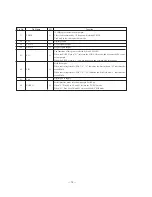
Input 384fs (16.9344MHz) or 768fs (33.8688MHz).
+5V power supply
Ground
CD-ROM decoder, audio decoder master clock. Input a clock to the XTL21 or connect an
oscillator between XTL2I and XTL2O. The recommended frequency is 45 MHz. This clock
is for the internal circuit. Does not synchronize with inputs and outputs.
+5V power supply
C2 pointer input
LR clock input
Summary of Contents for MCE-K700
Page 8: ... 8 ...
Page 9: ... 9 ...
Page 10: ... 10 ...
Page 11: ... 11 ...
Page 12: ... 12 ...
Page 13: ... 13 ...
Page 14: ... 14 ...
Page 15: ... 15 ...
Page 16: ... 16 ...
Page 21: ......
Page 22: ......
Page 23: ......
Page 24: ......
Page 25: ......
Page 26: ......
Page 27: ......

